
|
|
1.IntroductionDielectric photonic crystal (PC) slabs are a promising realization of PC by means of photonic bandgap in a plane and by index guiding in a vertical direction. Particularly, PC slab resonant cavities, created by introduction of defects into periodic structures, have recently attracted much attention due to their remarkable properties such as ultrasmall mode volume, high quality factor, and strong background suppression ability.1 They have shown great promise for a wide range of applications, including laser sources, sensors, nonlinear optics, computing, and quantum information processing. Generally, the thickness of the PC slab containing defect cavities needs to be chosen carefully to allow confining only a fundamental mode and preventing higher-order modes from fitting within the slab.2 The field intensity of the localized fundamental mode is typically maximal at the spatial center of the defect and decays exponentially toward the top and bottom surfaces of the defect. Thus, the highest intensity region of the defect-mode field in the slab is actually not exposed directly to the external environment. This may hinder the employment of the PC slab cavity for many emerging applications where strong interactions between optical fields and substances of interest are required on the device surface, e.g., sensors for detection of bio-species,3 tweezers for trapping of cells,4 imaging devices for near-field microscopy,5 and nano-opto-mechanical actuators.6 To overcome this issue, we devise to displace the localized defect-mode field of the PC slab cavity from the spatial center to the surface of the slab using a photonic-plasmonic integration scheme through the fusion of the slab cavity and an isolated metallic structure. Surface plasman resonance (SPR) is an effective subwavelength optical confinement approach to confining light to the interface between metal and dielectric with several orders of magnitude enhancement in field intensity.7 There have been many photonic-plasmonic integration schemes such as using metal strips on dielectric waveguides,7 suspending dielectric cylinders near metal surfaces,8 and coating continuous metals on dielectric PC slabs.9 These schemes usually use the guided mode in dielectric materials coupled to long-range propagating surface plasmons in metallic structures. They are promising to construct integrated chips that incorporate plasmonic structures and other optical components. But, because the guided mode is used, the field intensity contrast between the SPR mode in the metal and the guided mode in the background dielectric is relatively low. On the other hand, localized SPR (LSPR) usually uses free-space coupling of incident lights onto metallic structures such as nanoparticles, nanowires, nanoshells, and sharp tips.10 LSPR performs excellently in enhancing the field intensity contrast between metal and dielectric. But generally, there is lack of on-chip control and manipulation of excitation light at the subwavelength scale to suppress background fields around metallic structures. Also, integration of LSPR structures with other optical components remains challenging.10 As mentioned earlier, our devised photonic-plasmonic integration scheme is to use isolated metallic structures on the top surface of a missing-hole defect in a dielectric PC slab [Fig. 1]. By exciting the metal's SPR mode using the cavity's defect mode, the resonant field of the cavity can be spatially lifted up from the spatial center to the top surface of the slab. Here, the cavity acts to concentrate lateral incident lights to the defect, significantly minimizing the background field intensity around the metal. Therefore, a high field intensity contrast between the metal and surrounding dielectric can be rationally achieved. Due to the PC's notable capability to control and manipulate light, the devised scheme would potentially integrate with many other PC-based components (e.g., reflectors, waveguides, beam splitters, and switches) on a single photonic chip, permitting introduction of new functionalities and miniaturization of photonic devices. 2.Physical Model and Simulation MethodTo simulate the devised device structure, the PC slab was constructed by embedding an array of air columns in silicon (Si) substrate and a point defect was created by introducing a missing hole in the slab's center where a square-shape, thin silver metal film was located [Fig. 1]. Because design strategies to gain high-quality PC cavities have been widely reported elsewhere,11 a simple square lattice photonic structure was used to simplify computation while preserving the concept. The structural parameters were set as follows: the slab thickness h = a (a is the lattice constant), the air hole diameter d = 0.8 a, the metal thickness t = 0.025 a, and the side length of the silver square l = 0.5 a. The PC slab was periodically processed in both X and Z directions except the defect region. Our simulations utilized the three-dimensional plane-wave transfer matrix method (3D PWTMM).12 The periodic boundary condition was applied at the plane perpendicular to the direction of wave propagation. Perfectly matched layers were added to the simulation structure. The computing region covered five periods of the lattice in planar directions, and two identical air layers with a thickness of 5 a, each extending beyond the top and bottom surfaces of the slab. The incident light, with a y-polarized electric field, came laterally through a Si waveguide [not shown in Fig. 1] into the structure. The waveguide was connected at the input side of the slab [see Fig. 1]. Two identical perfectly matched layers with a thickness of 5 a each were placed on the top and bottom surfaces of the waveguide. The spatial grid was 3 nm in all directions. Optical parameters of the materials used in the simulations were all from Ref. 13. 3.Results and DiscussionsWe first examined the characteristic transmission spectrum of the PC slab cavity with no silver structure as a function of the normalized frequency f = a / λ. As shown in Fig. 2, the resulting cavity's photonic bandgap is located between f = 0.2 and 0.35 with the defect mode frequency at f = 0.2992. The lattice constant of a = 464 nm is thus suitable to support the telecommunication bandwidth (∼1550 nm). This cavity can produce a confinement of the fundamental defect mode with the quality factor of 102 and the −20 dB mode volume of 0.3087 μm3. The electric field distributions in Figs. 2, 2, 2 show that the defect-mode field at 1550 nm resides at the defect's spatial center. The maximum field intensity contrasts between the spatial center and planar directions [Fig. 2], and between the spatial center and vertical [Figs. 2, 2] directions are 85 and 120, respectively. The results show the cavity's ability to localize the defect-mode field and suppress the background field in the dielectric. The field intensity at the top surface is about four times lower than at the spatial center of the defect region. Fig. 2(a) Transmission spectrum of the PC cavity without the silver structure as a function of the normalized frequency. The inset shows a more detailed spectrum around the defect mode frequency of the cavity. (b) Schematic of the PC cavity used in the simulation. (c–e) Electric field (amplitude) distributions in the X-Z plane at the half height of the slab thickness y = − a/2 (c), in the X-Y plane at the cross-section A-A′ (d), and in the Y-Z plane at the cross-section B-B′ (e). 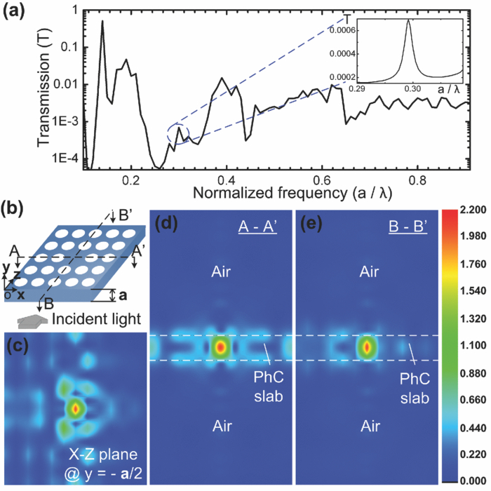 The devised isolated metal-on-PC slab cavity structure was then simulated [Fig. 3]. The incident light for this simulation was also chosen at λ = 1550 nm with y-polarized electric field. The transmission spectrum of this structure is presented in Fig. 3. As shown in Figs. 3, 3, 3, the SPR is indeed excited and localized in the silver square at 1550 nm. Because the majority of the defect-mode energy is transferred to the device surface due to the SPR excitation, the field intensity at the defect's spatial center is lowered. The energy transfer is also confirmed by the distinct drop in the transmission peak in Fig. 3 [compared to Fig. 2]. In comparison to the defect mode without the silver square in Figs. 2, 2, the −20 dB mode volume of the SPR is decreased to 0.0122 μm3 by a factor of 25 and the maximum field intensity at the defect surface is increased by a factor of 1.8. Furthermore, the maximum field intensity contrasts between the defect's surface and surrounding regions are increased from 85 [Fig. 2] to 110 by a factor of 1.3 in the planar directions [Fig. 3], and from 120 [Figs. 2, 2] to 180 by a factor of 1.5 in the vertical directions [Figs. 3 and 3]. Therefore, the devised structure cannot only couple the defect mode with the SPR mode to lift up the resonance field to the surface of the defect region, but also enhance the field intensity in a smaller mode volume. It should be pointed out that as shown in Figs. 2, 2, 2, 3, 3, 3, there exist some field coupling between the cavity and its neighboring cells. The coupling field intensity in these neighboring cells is actually weak, although we only used the simple, low-quality cavity in these simulations. Using high-quality cavities can reduce the coupling field around the cavity.11 Fig. 3(a) Transmission spectrum of the isolated metal-on-PC slab cavity structure as a function of the normalized frequency. The inset shows a more detailed spectrum around the defect mode frequency of the cavity. (b) Schematic of the isolated metal-on-PC slab cavity structure for simulation. (c–e) Electric field (amplitude) distributions in the X-Z plane at y = 0 (c), the X-Y plane at the cross-section C-C′ (d), and the Y-Z plane at the cross-section D-D′ (e) for the structure shown in (b). (f) Schematic of the silicon waveguide–metal counterpart structure for simulation. (g–i) Electric field (amplitude) distributions in the X-Z plane at y = 0 (g), the X-Y plane at the cross section E-E′ (h), and the Y-Z plane at the cross-section F-F′ (i) for the structure shown in (f).  To further reveal the benefit of the devised structure in terms of the field enhancement and the background suppression, we simulated a Si slab waveguide–metal counterpart [Fig. 3] for comparison. The structural parameters and boundary conditions of the counterpart were chosen the same as those used in Fig. 3, except no air holes were in the counterpart. As shown in Figs. 3, 3, 3, the SPR of silver is excited by the guided mode in the waveguide. The SPR field intensity, however, is approximately 1 order of magnitude less than that of the devised scheme owing to the low evanescent field intensity of the guided mode. The maximum field intensity contrasts between the silver and surrounding regions are only about 2 in the planar [Fig. 3] and 15 in the vertical [Figs. 3, 3] directions. This is because the counterpart is incapable of concentrating the guided-mode field under the isolated silver. On the contrary, the PC slab cavity can concentrate highly, the defect-mode field within the defect region, causing the increased SPR at the device surface; thus the improved ability to suppress background fields. The impacts of the major structural parameters (the slab thickness h and the silver thickness t) of the devised structure on the SPR wavelength λSPR and mode volume VSPR deserve discussion. Figure 4 shows that t has little influence on λSPR for a given h. As h varies from 232 nm (0.5 a) to 580 nm (1.25 a), λSPR is changed only slightly between 1530 and 1590 nm. This is because both the lattice and defect configurations of the PC remain unchanged. Another interesting observation is that VSPR reaches minimum at h = a in all cases for t ranging from 12 to 24 nm [Fig. 4]. The possible explanation for this observation is that VSPR may be dominated by the −20 dB mode volume of the defect mode VDEF, because VDEF is also found minimum at h = a [Fig. 4]. Fig. 4(a) Dependence of the coupled SPR mode wavelength λSPR on the slab thickness h for different metal thicknesses t. (b) Left y-axis: dependence of the volume of the coupled SPR mode VSPR on h for different t. Right y-axis: dependence of the volume of the defect mode of PC cavity VDEF without the metal (t = 0) on h. 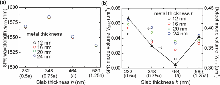 4.ConclusionThe uniqueness of the devised structure lies in using the defect mode of the PC slab cavity to excite the SPR mode of the isolated metallic structure on the top surface of the defect region. This photonic-plasmonic integration scheme allows lifting up the resonant field from the defect's spatial center to the defect surface, enhancing the strong interaction of optical fields with external substances at the device surface. Through the fusion between the PC slab cavity and the isolated metallic structure, this technology is relatively simple and highly adaptable, particularly as appropriate modifications to the device materials and geometries (e.g., dielectric, metal, lattice type, and defect geometry) and necessary integration with some of the many other PC-based components (e.g., mirrors, waveguides, splitters, filters, switches) should make it possible to meet various application requirements. More importantly, this devised photonic-plasmonic structure can provide direct open access for substances of interest to the strong field localized inside PC slabs, benefiting many applications that rely on strong light-object interactions. AcknowledgmentsThis work was supported by the U.S. DOE's Ames Lab Seed Fund, the DOE's Basic Energy Sciences Office through the Ames Lab, and the National Science Foundation under CAREER Award (ECCS 0954765). ReferencesY. Akahane, T. Asano, B. S. Song, and S. Noda,
“High-Q photonic nanocavity in a two-dimensional photonic crystal,”
Nature (London), 425 944
–947
(2003). http://dx.doi.org/10.1038/nature02063 Google Scholar
J. D. Joannopoulos, S. G. Johnson, J. N. Winn, and R. D. Meade, Photonic Crystals: Molding the Flow of Light, Princeton University Press, New Jersey
(2008). Google Scholar
J. Homola,
“Surface plasmon resonance sensors for detection of chemical and biological species,”
Chem. Rev., 108 462
–493
(2008). http://dx.doi.org/10.1021/cr068107d Google Scholar
A. N. Grigorenko, N. W. Roberts, M. R. Dickinson, and Y. Zhang,
“Nanometric optical tweezers based on nanostructured substrates,”
Nat. Photonics, 2 365
–370
(2008). http://dx.doi.org/10.1038/nphoton.2008.78 Google Scholar
E. Betzig and J. K. Trautman,
“Near-field optics: Microscopy, spectroscopy, and surface modification beyond the diffraction limit,”
Science, 257 189
–195
(1992). http://dx.doi.org/10.1126/science.257.5067.189 Google Scholar
M. Li, W. H. P. Pernice, C. Xiong, T. Baehr-Jones, M. Hochberg, and H. X. Tang,
“Harnessing optical forces in integrated photonic circuits,”
Nature (London), 456 480
–484
(2008). http://dx.doi.org/10.1038/nature07545 Google Scholar
W. L. Barnes, A. Dereux, and T. W. Ebbesen,
“Surface plasmon subwavelength optics,”
Nature (London), 424 824
–830
(2003). http://dx.doi.org/10.1038/nature01937 Google Scholar
R. F. Outon, V. J. Sorger, D. A. Genov, D. F. P. Pile, and X. Zhang,
“A hybrid plasmonic waveguide for subwavelength confinement and long-range propagation,”
Nat. Photon., 2 496
–500
(2008). http://dx.doi.org/10.1038/nphoton.2008.131 Google Scholar
F. Wu, D. Han, X. Hu, X. Liu, and J. Zi,
“Complete surface plasmon-polariton band gap and gap-governed waveguiding, bending and splitting,”
J. Phys.: Condens. Matter, 21 185010
(2009). http://dx.doi.org/10.1088/0953-8984/21/18/185010 Google Scholar
E. Hutter and J. H. Fendler,
“Exploitation of localized surface plasmon resonance,”
Adv. Mater., 16 1685
–1706
(2004). http://dx.doi.org/10.1002/adma.200400271 Google Scholar
D. Englund, I. Fushman, and J. Vuckovic,
“General recipe for designing photonic crystal cavities,”
Opt. Express, 13 5961
–5975
(2005). http://dx.doi.org/10.1364/OPEX.13.005961 Google Scholar
M. Li, Z. Y. Li, K. M. Ho, J. R. Cao, and M. Miyawaki,
“High-efficiency calculations for three-dimensional photonic crystal cavities,”
Opt. Lett., 31 262
–264
(2006). http://dx.doi.org/10.1364/OL.31.000262 Google Scholar
E. D. Palik, Handbook of Optical Constants of Solids, Academic Press, Orlando, FL
(1985). Google Scholar
|


