
|
|
1.IntroductionPorous silicon optical films produced by the electrochemical etching of silicon1 present an attractive means of creating a film with multiple tunable optical features. The current density applied during the etch process determines the porosity-depth profile and the resulting refractive index profile of the film with depth, allowing a variety of optical structures to be programed into the material. Structures including Bragg stacks,2, 3 Fabry–Pérot layers,2 and single and multiple stopband rugates3, 4 have been widely produced and applied to gas sensing in the visible and near-infrared (NIR) region of the spectrum. Rugate structures contain a sinusoidal refractive index variation with depth. Multiple sinusoids can be combined into composite profiles that display stop bands corresponding to each component frequency.4, 5 This work demonstrates the use of an electrochemically prepared porous Si-based optical filter to optically sense target molecules at medium-wave infrared (MWIR) wavelengths by matching the reflectance spectrum of the porous Si layer to the infrared absorption bands of target molecules (CO2 and P=O species in this work). The CO2 detector uses a rugate filter tuned to match the principal νCO2 stretching mode of carbon dioxide at 2350 cm−1.6, 7 Typically, spectral imaging systems detect CO2 at NIR wavelengths like 2.05 μm due to the availability of sensitive detectors in this wavelength range,8 but as a proof of principle the 4.2 μm MWIR absorption band was utilized here. A composite filter based on the superposition of two sinusoid frequencies was also constructed to create a structure that incorporates a tunable reflectance reference channel. In order to demonstrate the ability to fabricate infrared reflection features at the edge of the long-wave infrared region, a filter was constructed with an optical peak at 1250 cm−1 (8 μm), the wavelength of the P=O bond vibration in the G-series chemical warfare agents soman, sarin, tabun, and VX.9, 10 In recent years, porous silicon structures prepared as optical rugates in the infrared region of the spectrum have primarily focused on the near infrared, particularly at telecommunications wavelengths for applications such as broadband mirrors and switches.3, 11, 12 Some sensing work at NIR wavelengths has been performed, with Chapron applying NIR rugates in the 1–3 μm region to directly detect liquid analytes with the porous matrix.13 Because NIR structures require shorter spacing of the dielectric layers and, thus, thinner films than those required for medium and long wave infrared filters, they are less affected by electrochemical fabrication issues of electrolyte diffusion and depletion that can occur at long etch times. Typical methods to prepare MWIR filters, such as chemical vapor deposition,14 glancing angle deposition,15 and thermal evaporation16, 17 are slow and costly. MWIR optical structures pose additional fabrication challenges, but there is a significant need for infrared hyperspectral imaging systems and filters for two-dimensional infrared imaging that make up the low-cost, rapid electrochemical fabrication method used to prepare porous Si desirable. Recently, Ishikura fabricated MWIR porous silicon structures at 5–10 μm, demonstrating the ability to create broadband high-pass filters,18 and Lo and Murphy have demonstrated fabrication of rugate filters with broad stop bands at terahertz frequencies.19 In contrast, the aim of this work is to create narrowband spectral features that overlap the vibrational bands of gas-phase molecules and to demonstrate the application of these structures to free-space infrared gas sensing using a reflectance-mode filter with a MWIR detector. The large planar surface area of the porous Si filter (1.2 cm2 in this study) motivates their application as optical filters for 2-D infrared imaging, because the filters are sufficiently large enough to cover the imaging field. In the NIR, 2-D imaging has been used for applications including counterfeit pharmaceutical detection20 and hyperspectral microscopy. In the MWIR, imaging is of interest for satellite remote imaging21 and remote sensing,22 as well as military applications in airborne surveillance, target detection and tracking, and thermal imaging. The ability to acquire 2-D infrared images was developed in the 1970s, and a variety of detection materials, such as vanadium oxide bolometers and barium strontium titanate detectors, have employed.23 In the past decade, quantum-dot infrared photodetectors24 (QDIPs) and quantum-well infrared photodetectors (QWIPs) have enabled cameras with megapixel resolution.25 Ordered photonic structures have even been used for infrared detection,26 but the work presented here aims not to capture infrared photons with porous Si photonic crystals but rather to complement existing imaging detectors with a passive porous Si filter element. Porous Si can be tailored to exhibit sharp spectral features.27 In contrast, recent developments with voltage tunable multiband infrared focal plane arrays using MEMS technology23 to create tunable infrared filters has resulted in broadband structures that are not suitable to sensing specific chemical species by matching molecular vibrational absorption bands. This work represents the first example of a porous Si spectral filter prepared to match specific spectral features of molecules in the MWIR (fingerprint) region. Although the ability of the filters to restrict specific optical wavelengths makes them an attractive material to couple with broadband infrared detectors [such as a forward-looking infrared camera], a narrowband, high-resolution Fourier-transform infrared (FTIR) spectrometer was employed in the present study in order to quantify the spectral characteristics of the porous Si filters. FTIR is widely used for sensing chemical agents28 and forensic chemical imaging, with a single scan providing a spectrum analogous to a single pixel in a hyperspectral infrared imaging system.29 2.Experimental Setup2.1.Fabrication of Optical StructuresPorous Si samples were prepared from single-crystal, (100)-oriented highly boron-doped p-type Si (Siltronix, Archamps, France, 0.92 mΩ cm resistivity) by electrochemical etching in a 3:1 v:v solution of aqueous hydrofluoric acid (HF) to ethanol (49% hydrofluoric acid from Fisher Scientific, Inc., Pittsburgh, PA, USA). Etching was performed in a Teflon® cell with a platinum mesh counter electrode and a galvanostat (Kepco, Inc., Flushing, NY, USA, BOP 50–4D) under computer control (LabView, National Instruments, Austin, TX, USA). Single- and composite-frequency rugate etches were fabricated with a current waveform varying between 25 and 100 mA/cm2, applied nominally for 45 cycles with other sinusoid conditions as indicated. Fresh HF was introduced to the etch cell during electrochemical fabrication by replacing 1.5 mL of the 3:1 etch solution at 5-min intervals. Lifted-off porous films for use in FTIR transmission mode were achieved by detaching the porous layer from the bulk Si wafer with an electropolishing current of 2.7 mA/cm2 for 5 min in a 3.3% HF:ethanol solution. Rugate etch currents varied as a function of time t, according to where where Imax and Imin are the high and low currents, and p is the period of component i in seconds. For single-frequency rugates, n = 1. The composite rugate described later contained n = 2 components with periods p1 and p2.2.2.Gravimetric Determination of PorositySamples were weighed before etching (m1), after etching (m2), and after dissolving the porous layer with a 0.1-M basic solution of KOH in water and rinsing with ethanol (m3). The following equation was used to determine the porosity:30 2.3.Infrared SpectroscopySpectra were recorded with a Thermo Scientific Nicolet 6700 FTIR with an MCT/A detector and KBr beam splitter using a resolution of 2 cm−1 and an average of 128 scans. Attenuated total reflectance (ATR) spectra were acquired with a smart iTR diamond accessory. Transmission-mode spectra were acquired by mounting the lifted-off porous Si film between two KBr circular plates (Koch Crystal, Elyria, OH, USA) and placing the assembly on a transmittance accessory stage normal to the infrared beam. Reflectance-mode spectra were acquired with a beam-deflector setup as pictured in Fig. 1 and with filters that were not lifted off from the bulk underlying Si. Four Ag mirrors (Thorlabs, Newton, NJ, USA), mounted on posts and positioned at a specular angle of 12.5 deg, diverted the beam path through a gas sample cell. The 2.5-in-long glass gas cell was positioned in the beam path as depicted and used KBr windows and had Swagelok input and output ports. Reference spectra were taken by replacing one mirror, on the detector side of the gas cell, with polished Si. Sample spectra were taken by replacing the polished Si with a porous Si sample. A flow of ∼2 L/min of nitrogen, measured with a mass flow controller (Alicat Scientific, Tucson, AZ, USA) was passed through the gas cell. Spectral acquisitions with CO2 were taken by first purging the cell with a 2-L/min flow of CO2 for 5 min, with continuous flow during sampling. Fig. 1Schematic view of the reflectance-mode gas-sensing configuration used. The source and detector are from a conventional FTIR instrument. Silver mirrors divert the beam (arrows) through a gas cell with KBr windows. The porous silicon optical structure (pSi) is mounted at one of the beam-deflection locations, as pictured. A reference spectrum is acquired with a polished silicon chip mounted in the pSi location. 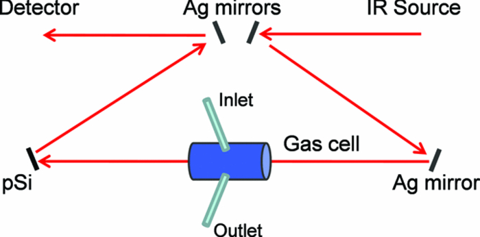 2.4.Effectical Optical Thickness DeterminationReflectance spectra of the samples in the visible region were taken across 530–1200 nm with a CCD spectrometer (Ocean Optics, Dunedin, FL, USA, USB4000) and a tungsten-halogen light source (Ocean Optics LS-1) connected with a Y-branch bifurcated optical fiber. The common end of the bifurcated fiber was focused with an objective lens to a 2-mm2 spot size and positioned normal to the porous silicon sample surface. A routine using a fast Fourier transform (FFT) of the optical interference fringes in the visible between 850 and 1000 nm was used to determine the effective optical thickness (EOT) (2 nL) of the layers.31 2.5.Scanning Electron MicroscopyPorous silicon layer thickness was determined by cutting and imaging cross sections of the filters with an FEI XL30 SFEG scanning electron microscope (SEM) in ultra high-resolution mode with a through lens detector at 10 kV without prior metallic sputtering of the sample. 3.Results and Discussion3.1.Porous Si Rugate Filters with Medium-Wavelength Infrared Spectral FeaturesA comparison of spectra from three FTIR acquisition configurations for a filter with a sinusoidal current-time waveform period of p = 60 s is shown in Fig. 2. In all configurations, spectral bands corresponding to the filter material are observed. The filters in this study were designed with resonant peaks outside of the bands corresponding to the Si–H vibrational signatures of the freshly prepared filters. Oxidation of the filters by aging in air will introduce spectral bands corresponding to Si–O and Si–OH bonds that must also be avoided. Spectra obtained in the ATR configuration clearly exhibit features of the fresh Si–H surface, with ν(SiHx) stretches at 2112 and 2087 cm−1, δ(SiH2) at 907 cm−1, and δ(SiHx) at 623 cm−1. No rugate stop band feature is visible under ATR due to the limited depth of penetration of the infrared beam into the filter layer relative to the physical thickness of the rugate cycles. Fig. 2Comparison of three FTIR acquisition modes and resulting spectra for an infrared rugate optical structure with a sinusoid etching wave period of 60 s. (a) Attenuated total reflectance. (b) The optical structure was lifted off from the bulk and the spectrum acquired in transmission mode. (c) Reflection-mode interrogation using the beam diversion configuration in Fig. 1. The percent reflectivity is relative to a polished Si reference sample. 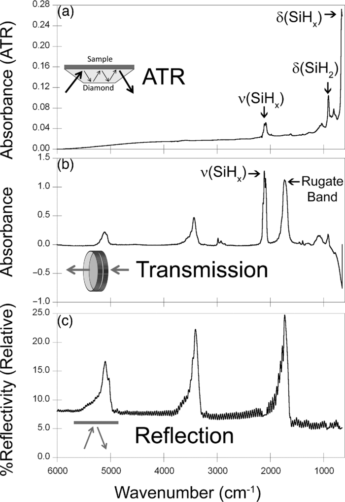 In the transmission configuration, the ν(SiHx) stretching vibration is very strong, since the light is absorbed in that band as it passes through the optical film. The principal rugate band at 1715 cm−1 is observed, as well as higher order harmonics at 2/λ and 3/λ.4 If desired, these higher order harmonics may be suppressed by creating filters with a sinusoidal modulation of the logarithm of the refractive index n with depth3, 18 rather than a direct sine variation of n. Here, the 2/λ band was desired and utilized as an optical reference channel. The thickness of the filter balances a trade-off between increasing the number of sinusoid repetitions to reduce thin-film interference fringes and increasing the material's absorbance in the Si–H bands outside of the desired rugate spectral position. To sense absorbing molecules in the beam path, a reflection rather than transmission configuration is desirable. In reflection mode, an absorbing gas is sensed as a reduction in peak reflectivity, while in transmission mode the absorbing gas results in a slight decrease in the already low filter transmittance of the rugate band. The spectrum in Fig. 2 obtained in the reflection configuration clearly exhibits the rugate reflection band as well as higher order harmonics at 2/λ and 3/λ, with the Si–H stretches of the material's absorbance appearing as reductions in the reflectivity at ∼2100 cm−1. Thin-film interference fringes are present due to reflections from the top and bottom interfaces of the optical structure, where the bottom interface consists of the porous Si layer and bulk silicon. Despite mounting the porous Si sample at a 15-deg angle of incidence, the center wavenumber of the rugate band at 1742 cm−1 in the reflectance configuration was only slightly lower than its appearance at 1730 cm−1 in the transmission configuration, where the filter was normal to the incident beam. This is not surprising because, for an incident angle θ0, the wavelength of the peak at an angle θ relative to its location at normal incidence (λ0) is given by:12 Eq. 4[TeX:] \documentclass[12pt]{minimal}\begin{document}\begin{equation} \lambda _\theta = \lambda _0 \cos (\theta _{\rm a}) = \lambda _0 \left( {1 - \frac{{\sin ^2 \theta _0 }}{{n_{{\rm avg}} ^2 }}} \right)^{1/2}, \end{equation}\end{document}3.2.Effect of Rugate RepetitionsIncreasing the number of sinusoid etch repetitions for a given fixed period reduces the height of the thin layer interference fringes relative to the rugate peak while increasing the etch thickness. Thicker layers result in increased absorption at porous Si–H absorption frequencies. For the gas-sensing work above, layers with 45 rugate cycles were chosen as a nominal value exhibiting acceptable thin-film fringe reduction. Figure 3 displays spectra taken in reflectance mode of four etches with varying numbers of rugate cycles for a period of p = 43.7 s. The effective optical thickness (2navgL) increases linearly with the number of cycles due to the linear increase in the layer thickness L, for the constant average layer refractive index navg. This result indicates that issues affecting the etch rate of the porous layer do not dramatically deviate the linearity of the optical thickness with total etch time for very thick (>50 μm) etches.32 Specifically, the diffusion of the HF electrolyte into the increasingly thicker film during long etches does not appear to have limited the etch rate. Fig. 3(a) Effect of the number of sine wave cycles on the reflectivity spectrum, for an optical structure with a period of 43.7 s. (b) Linear relationship between the effective optical thickness (2navgL, determined from the interference fringes apparent in the visible portion of the reflectance spectrum), and the number of sine wave cycles. 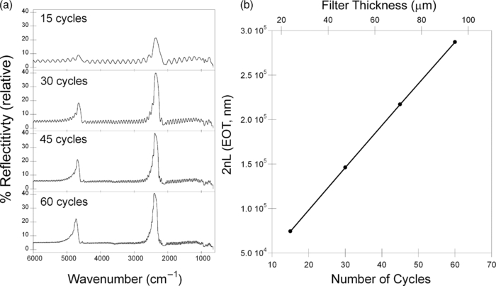 3.3.Effect of the Etching PeriodThe period of the current-time etch wave, given in Eq. 2, corresponds directly to the spectral position of the rugate band, and rugates with spectral bands across the MWIR have been created. Figure 4 displays reflectance FTIR spectra of several of these filters. Fig. 4Comparison of a series of etches with constant total etching times but with (a) a variable number of cycle repetitions to a series of etches with a constant number of sinusoid cycle repetitions but (b) with variable etching times. Spectra from structures of four of the sine-wave periods in each series are shown. The total etch time was equal to the period times (in seconds) the number of cycles. The two calibrations coincide at p = 50 s, where each consisted of 45 repetitions and a total etch time of 2250 s.  The periodic variation of the current density with time given in Eq. 2 results in a periodic variation of the refractive index with depth z, expressed as3, 4 Eq. 5[TeX:] \documentclass[12pt]{minimal}\begin{document}\begin{equation} n(z) = n_{{\rm avg}} + \frac{{\Delta n_{{\rm avg}} }}{2}\sin \left( {\frac{{4\pi n_{{\rm avg}} z}}{{\lambda _0 }}} \right) = n_{{\rm avg}} + \frac{{\Delta n}}{2}\sin \left( {\frac{{2\pi z}}{d}} \right), \end{equation}\end{document}Figure 4 compares two sets of period versus peak wavelength (λ0) calibrations of MWIR porous Si filters, one in which the total etch time was held constant and the number of cycles varied [Fig. 4], and the other in which the number of sinusoid cycles was held constant and the total etch time varied [Fig. 4]. The two calibration series share a coincident point at a sine period of p = 50 s. As expected, the etches with a constant total etch time have a similar spacing between the thin-film interference fringes, while the increasing thickness, and therefore optical thickness, of the constant-cycle etches results in a corresponding decrease in fringe spacing. Figure 5 displays the effective optical thickness (EOT, 2navgL) and rugate peak position of these etches versus the period. The EOT was determined by an FFT of the thin-layer interference fringes in the visible spectrum. EOT values based on FFT of fringes in the infrared were also calculated and differed by a constant −4% from the visible values obtained at normal incidence. The filters with a constant total etch time display a slight decrease in effective optical thickness with the increasing period, in contrast to the linearly increasing EOT with period for constant-cycle, variable-etch-time filters, shown in Fig. 5. The EOT scales linearly with the period since for a constant navg of the layer, the thickness L is a direct function of the etch rate (in nanometers/second) multiplied by the etch time (in seconds). The rugate peak position of both the constant-time and constant-repeat etches is linear with etch period, as shown in Fig. 5. This is expected because λ0 scales with the period p, and thus, the quantity 1/λ0 should scale with the frequency, 1/p. Additional etches that were performed separately from the two trials above are included in Fig. 5 and show excellent agreement with these trends. Fig. 5(a) Effective optical thickness versus the etchwave period for porous Si optical filters. Filters fabricated with a constant total etching time (π) are compared to those etched for a constant number of sinusoid cycles (● and ■). (b) Position of the principal rugate spectral peak as a function of the frequency (1/period) for both constant-time and constant-cycle repetition calibrations.  Several issues can affect the etch rate for longer etches and, consequently, the value of EOT and the spectral peak positions. HF diffusion to the etching boundary for thick layers can lead to a decrease in the layer growth rate with depth, and a reduction of the concentration of HF as it is consumed can influence the etch rate of long-duration etches with low electrolyte volumes.1, 32 To address this, the volume of HF was mixed and partially replaced every 5 min during an etching procedure. Incorporation of etch stops for 1 s every cycle to allow equilibration of electrolyte concentration showed no difference in optical properties or layer thickness, though others have utilized shorter etch stops to homogenize electrolyte distribution when creating ∼300-μm-thick rugate filters with stop bands at terahertz frequencies.19 Furthermore, after a section of the filter has been electrochemically etched, it will continue to dissolve at a much lower rate while in contact with HF, leading to a high- to low-porosity gradient from the top to bottom of the etched layer. The linearity of the EOT and peak position in Fig. 5 with increasingly thicker etches and longer etch times (increasing periods for constant cycles) indicate that these issues were not significant for the samples under investigation here. The gravimetric porosity was determined for all etched layers as 74%, with no more than a ±1% variation across all samples, attributable to error in the weighing of the samples. The porosity exhibited no trend with changes in period, indicating uniformity of the etch rate with increasing etch time of the samples. It is also worth noting the decrease in the width of the rugate peaks in the FTIR spectra with increasing period. This is an expected result of changing the reflectance band position because the width of the spectral band Δλ centered at λ0 can be expressed as12, 34 Eq. 6[TeX:] \documentclass[12pt]{minimal}\begin{document}\begin{equation} \frac{{\Delta \lambda }}{{\lambda _0 }} = \frac{{\Delta n}}{{2n_{{\rm avg}} }}. \end{equation}\end{document}The SEM thickness and effective optical thickness (2navgL) of a filter specimen can be used to determine the average refractive index navg of the porous filter For the single-peak CO2 sensor example with a thickness of 70.7 μm, navg = 1.51. The refractive index of the silicon pillars in the porous material, nSi, was then determined as 3.67 using the two-component Bruggeman effective medium approximation,33 using a value of EOT determined from the optical interference spectrum between 850 and 1000 nm. This is a close match to the literature value of n = 3.6 at 900 nm.35 This agreement indicates that the optical properties of the filters tuned to MWIR wavelengths are consistent with expected porous silicon properties. 3.4.Demonstration of Gas Sensing with a Single-Peak RugateA rugate filter tuned to the ν(CO2) band is shown in Fig. 6. The CO2 vibrational bands between 2260 and 2390 cm−1 are easily observed in a reference sample of the gas taken without the porous Si filter by using silver mirrors at all beam deflection locations. The slight sawtoothing visible around 2350 cm−1 is due to incompletely resolved Q and R absorption branches (FTIR resolution was 2 cm−1). The absorptions at higher wavenumbers are the result of combination vibrational modes, with a doublet at 2.7 μm and higher members of the same sequence at 2.0 μm.6, 7 The signals observed from 1400 to 1800 cm−1 is due to a small amount of residual water vapor in the FTIR chamber. Fig. 6Reflectance-mode FTIR spectra demonstrating a porous Si rugate filter containing an in-band and an out-of-band peak for detection of CO2. The rugate was etched with a single-frequency sinusoidal current-time waveform with a period p = 43.7 s. (a) Gas chamber purged with CO2, with silver mirrors mounted in all four beam deflection locations (see Fig. 1). (b) Gas cell purged with N2, with porous Si filter mounted at the deflection position indicated in Fig. 1. The sample was prepared such that one of the stop-band resonances appears at ∼2300 cm−1, coinciding with the C–O stretching band of CO2. The other peak (at ∼4600 cm−1) is an overtone band. (c) Gas cell purged with CO2, with porous Si at the beam deflection position indicated in Fig. 1. 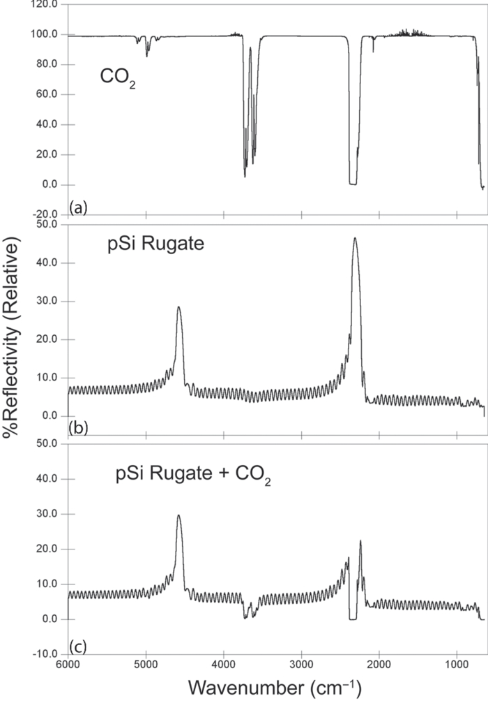 The rugate filter displayed in Fig. 6 was constructed with a current-time sinusoid waveform with a period of 43.7 s etched for 45 repetitions, designed to match the 2350 cm−1 principal absorption band. The resulting filter exhibited a cross-sectional thickness of 70.7 μm. On introduction of CO2 to the gas cell, the principal rugate band was obscured by the absorbing molecules, decreasing the peak area, while the higher order harmonic was unchanged. The ratio of the areas or of the intensities of the principal peak to the harmonic overtone peak can thus be used as a referenced sensor for the presence of CO2. 3.5.Gas Sensing with a Composite RugateIn the single-peak rugate described earlier, a harmonic band was utilized as a reference channel for the principal rugate band at 2350 cm−1 that overlaps the CO2 absorptions. The location of the harmonic band is spectrally distant from the principal peak and its location depends on the principal peak location. To introduce a tunable reference peak that is spectrally closer to the principal band, a composite, infrared rugate was fabricated consisting of a single layer combining two sinusoidal current-time frequencies into the current-time etch wave, as pictured in Fig. 7. Filters of each single frequency were fabricated for reference [Fig. 7], with the composite filter comprised of p = 43.7 s and p = 51 s periods that resulted in rugate bands at 2350 and 2000 cm−1 respectively, with a total layer thickness of 72.5 μm determined by SEM. As shown in Fig. 7, the presence of CO2 in the gas cell greatly reduced the area of the peak at 2350 cm−1, while not affecting the reference channel at 2000 cm−1. Figure 7 also demonstrates sensing of CO2 at lower concentrations. A spectrum reflected off the filter was taken for a 50/50 volumetric mixture of CO2 and N2 in the gas cell, as well as ambient room air. The reflectance scan of the latter exhibits a slight reduction in the 2350 cm−1 peak area and shows evidence of water vapor outside the rugate bands. Fig. 7Reflectance-mode FTIR detection of CO2 using a multi-frequency rugate optical filter. (a) Single-frequency components with p = 43.7 s (middle) and p = 51 s (bottom) compared to the composite filter (top). (b) Spectra of the composite filter with varying levels of CO2 in the gas sample cell: fully purged with CO2 (top), 50% CO2/50% N2 (middle), and an ambient level of CO2 from room air (bottom). 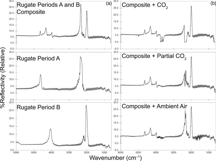 3.6.Matching P=O Bond Stretching ModesTo demonstrate the ability to tune rugate peaks to the edge of the long-wave infrared region, a filter was constructed to match a typical P=O stretching vibration at 1250 cm−1. This transition is present in the G-series chemical nerve agents sarin, soman, tabun, and VX.9, 10 The filter shown in Fig. 8 was etched with a sinusoid current-time period of p = 82.5 s, resulting in a 123-μm-thick layer as determined by SEM. Several overtone bands are clearly present. 4.ConclusionsOptical rugate filters with reflectance bands in the medium-wave infrared were successfully fabricated from porous silicon and used to detect CO2, by matching the reflectance peak to a vibrational absorbance band of the molecule. Filters with rugate bands tuned across the MWIR region were fabricated, including porous layers with an optical band at the wavelength of a typical P=O bond stretch at 1250 cm−1, and the spectral position of the sensing layer reflectivity band in the infrared exhibited excellent linearity with the frequency of the current-time sinusoid etching waveform. AcknowledgmentsThis material is based on work supported by the National Science Foundation under Grant No. DMR-0806859. ReferencesL. Canham, Properties of Porous Silicon, 1
–405 Short Run Press Ltd., London
(1997). Google Scholar
A. Janshoff, K. P. S. Dancil, C. Steinem, D. P. Greiner, V. S. Y. Lin, C. Gurtner, K. Motesharei, M. J. Sailor, and M. R. Ghadiri,
“Macroporous p-type silicon Fabry-Perot layers. Fabrication, characterization, and applications in biosensing,”
J. Am. Chem. Soc., 120 12108
–12116
(1998). http://dx.doi.org/10.1021/ja9826237 Google Scholar
E. Lorenzo, C. J. Oton, N. E. Capuj, M. Ghulinyan, D. Navarro-Urrios, Z. Gaburro, and L. Pavesi,
“Porous silicon-based rugate filters,”
Appl. Opt., 44 5415
–5421
(2005). http://dx.doi.org/10.1364/AO.44.005415 Google Scholar
W. E. Johnson and R. L. Crane,
“Introduction to rugate filter technology,”
Proc. SPIE, 2046 88
–108
(1993). http://dx.doi.org/10.1117/12.163554 Google Scholar
S. O. Meade, M. S. Yoon, K. H. Ahn, and M. J. Sailor,
“Porous silicon photonic crystals as encoded microcarriers,”
Adv. Mater., 16 1811
–1814
(2004). http://dx.doi.org/10.1002/adma.200400713 Google Scholar
P. E. Martin and E. F. Barker,
“The infrared absorption spectrum of carbon dioxide,”
Phys. Rev., 41 291
–303
(1932). http://dx.doi.org/10.1103/PhysRev.41.291 Google Scholar
R. C. Herman,
“Vibrational energy levels of the carbon dioxide molecule,”
Astrophys. J., 107 386
–388
(1948). http://dx.doi.org/10.1086/145022 Google Scholar
V. Zeninari, A. Vicet, B. Parvitte, L. Joly, and G. Durry,
“In situ sensing of atmospheric CO2 with laser diodes near 2.05 mu m: A spectroscopic study,”
Infr. Phys. Tech., 45 229
–237
(2004). http://dx.doi.org/10.1016/j.infrared.2003.11.004 Google Scholar
M. T. Soderstrom and R. A. Ketola,
“Identification of nerve agents and their homologs and dialkyl methylphosphonates by gas-chromatography-Fourier-transform infrared spectrometry (GC-FTIR). 1. spectral interpretation,”
Fres. J. Anal. Chem., 350 162
–167
(1994). http://dx.doi.org/10.1007/BF00323181 Google Scholar
E. H. Braue and M. G. Pannella,
“FT-IR analysis of chemical warfare agents,”
Mikrochim. Acta, 1 11
–16
(1988). http://dx.doi.org/10.1007/BF01205828 Google Scholar
M. Deubel, G. Von Freymann, M. Wegener, S. Pereira, K. Busch, and C. M. Soukoulis,
“Direct laser writing of three-dimensional photonic-crystal templates for telecommunications,”
Nat. Mater., 3 444
–447
(2004). http://dx.doi.org/10.1038/nmat1155 Google Scholar
A. G. Imenes and D. R. McKenzie,
“Flat-topped broadband rugate filters,”
Appl. Opt., 45 7841
–7850
(2006). http://dx.doi.org/10.1364/AO.45.007841 Google Scholar
J. Chapron, S. A. Alekseev, V. Lysenko, V. N. Zaitsev, and D. Barbier,
“Analysis of interaction between chemical agents and porous Si nanostructures using optical sensing properties of infra-red Rugate filters,”
Sens. Actuat. B, 120 706
–711
(2007). http://dx.doi.org/10.1016/j.snb.2006.03.038 Google Scholar
P. L. Swart, P. V. Bulkin, and B. M. Lacquet,
“Rugate filter manufacturing by electron cyclotron resonance plasma-enhanced chemical vapor deposition of SiNx,”
Opt. Eng., 36 1214
–1219
(1997). http://dx.doi.org/10.1117/1.601281 Google Scholar
K. Robbie, A. J. P. Hnatiw, M. J. Brett, R. I. MacDonald, and J. N. McMullin,
“Inhomogeneous thin film optical filters fabricated using glancing angle deposition,”
Electron. Lett., 33 1213
–1214
(1997). http://dx.doi.org/10.1049/el:19970834 Google Scholar
W. J. Gunning, R. L. Hall, F. J. Woodberry, W. H. Southwell, and N. S. Gluck,
“Codeposition of continuous composition rugate filters,”
Appl. Opt., 28 2945
–2948
(1989). http://dx.doi.org/10.1364/AO.28.002945 Google Scholar
K. Kaminska, T. Brown, G. Beydaghyan, and K. Robbie,
“Vacuum evaporated porous silicon photonic interference filters,”
Appl. Opt., 42 4212
–4219
(2003). http://dx.doi.org/10.1364/AO.42.004212 Google Scholar
N. Ishikura, M. Fujii, K. Nishida, S. Hayashi, and J. Diener,
“Porous silicon based extended-bandwidth rugate filters for mid-infrared application,”
Infr. Phys. Tech., 53 292
–294
(2010). http://dx.doi.org/10.1016/j.infrared.2010.04.005 Google Scholar
S. Z. A. Lo and T. E. Murphy,
“Nanoporous silicon multilayers for terahertz filtering,”
Opt. Lett., 34 2921
–2923
(2009). http://dx.doi.org/10.1364/OL.34.002921 Google Scholar
G. Sando and J. Dubois,
“Seeing” the chemicals in pharmaceutical tablets with NIR chemical imaging,”
Chim. Oggi-Chem. Today, 28 40
–42
(2010). Google Scholar
A. F. H. Goetz and B. Curtiss,
“Hyperspectral imaging of the Earth: Remote analytical chemistry in an uncontrolled environment,”
Field Anal. Chem. Tech., 1 67
–76
(1996). http://dx.doi.org/10.1002/(SICI)1520–6521(1996)1:2<67::AID-FACT2>3.0.CO;2-B Google Scholar
A. I. Dsouza, L. C. Dawson, E. J. Anderson, A. D. Markum, W. E. Tennant, L. O. Bubulac, M. Zandian, J. G. Pasko, W. V. McLevige, D. D. Edwall, J. W. Derr, and J. E. Jandik,
“VSWIR to VLWIR MBE grown HgCdTe material and detectors for remote sensing applications,”
J. Electron. Mater., 26 656
–661
(1997). http://dx.doi.org/10.1007/s11664–997-0211–8 Google Scholar
A. Rogalski, J. Antoszewski, and L. Faraone,
“Third-generation infrared photodetector arrays,”
J. Appl. Phys., 105 091101
(2009). http://dx.doi.org/10.1063/1.3099572 Google Scholar
A. D. Stiff-Roberts,
“Quantum-dot infrared photodetectors: a review,”
J. Nanophoton., 3 031607
(2009). http://dx.doi.org/10.1117/1.3125802 Google Scholar
S. D. Gunapala, S. V. Bandara, J. K. Liu, J. M. Mumolo, D. Z. Ting, C. J. Hill, J. Nguyen, B. Simolon, J. Woolaway, S. C. Wang, W. P. Li, P. D. LeVan, and M. Z. Tidrow,
“Demonstration of megapixel dual-band QWIP focal plane array,”
IEEE J. Quant. Electron., 46 285
–293
(2009). http://dx.doi.org/10.1109/jqe.2009.2024550 Google Scholar
J. M. Xu,
“Highly ordered carbon nanotube arrays and IR detection,”
Infr. Phys. Tech., 42 485
–491
(2001). http://dx.doi.org/10.1016/S1350–4495(01)00102–5 Google Scholar
S. Ilyas, T. Bocking, K. Kilian, P. J. Reece, J. Gooding, K. Gaus, and M. Gal,
“Porous silicon based narrow line-width rugate filters,”
Opt. Mater., 29 619
–622
(2007). http://dx.doi.org/10.1016/j.optmat.2005.10.012 Google Scholar
L. M. Shao, C. W. Roske, and P. R. Griffiths,
“Detection of chemical agents in the atmosphere by open-path FT-IR spectroscopy under conditions of background interference: I. High-frequency flashes,”
Anal. Bioanal. Chem., 397 1511
–1519
(2010). http://dx.doi.org/10.1007/s00216–010-3690-z Google Scholar
M. Tahtouh, J. R. Kalman, C. Roux, C. I. Lennard, and B. J. Reedy,
“The detection and enhancement of latent fingermarks using infrared chemical imaging,”
J. Forens. Sci., 50 64
–72
(2005). http://dx.doi.org/10.1520/JFS2004213 Google Scholar
A. Halimaoui,
“Porous silicon formation by anodisation,”
Properties of Porous Silicon, 12
–22 Short Run Press Ltd., London
(1997). Google Scholar
C. Pacholski, M. Sartor, M. J. Sailor, F. Cunin, and G. M. Miskelly,
“Biosensing using porous silicon double-layer interferometers: Reflective interferometric Fourier transform spectroscopy,”
J. Am. Chem. Soc., 127 11636
–11645
(2005). http://dx.doi.org/10.1021/ja0511671 Google Scholar
V. Lehmann, Electrochemistry of Silicon, 51
–75 Wiley-VCH, Weinheim, Germany
(2002). Google Scholar
M. S. Salem, M. J. Sailor, T. Sakka, and Y. H. Ogata,
“Electrochemical preparation of a rugate filter in silicon and its deviation from the ideal structure,”
J. Appl. Phys., 101 063503
(2007). http://dx.doi.org/10.1063/1.2710339 Google Scholar
H. A. Abusafia, A. I. Alsharif, and I. O. Abualjarayesh,
“Rugate filter sidelobe suppression using half-apodization,”
Appl. Opt., 32 4831
–4835
(1993). http://dx.doi.org/10.1364/AO.32.004831 Google Scholar
E. D. Palik, Handbook of Optical Constants of Solids, 337 Academic Press, New York
(1998). Google Scholar
|


