|
|
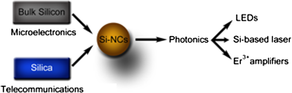
1.IntroductionIt is fair to say silicon and its passivating oxide have long been the workhorse materials for the electronics industry and more specifically integrated circuits (ICs). Similarly, silica fibre optics are the medium of choice for efficiently transmitting optical data over long distances. Based solely on material platform compatibility, one might expect substantial interconnect between these two dominant technological sectors; surprisingly, little exists. One of the primary reasons for this separation is the absence of a cost-effective light source compatible with silicon and silicon oxide. If such a light source could be realized, it could facilitate substantial advances that could address challenges associated with miniaturization of microelectronics. For example, very soon the copper interconnects within modern microprocessors will be unable to handle data transmission rates approaching 10 billion bits per second that will soon be required of them.1 If copper interconnects were replaced by silica optical structures and electrons supplanted by photons, data transfer rates approaching 100 billion bits per second are predicted.1 While the most obvious and straightforward light-emitting material should be silicon, unlike many semiconductors, its indirect bandgap limits its luminescence at room temperature. In this regard, the promise of integrated silicon electronics and photonics came very rapidly after Canham’s first report of photoluminescent porous silicon (p-Si).2 Luminescence from this landmark material arises from recombination of quantum confined carriers in small crystallites (or quantum dots) within the pores. Since then, many reports have followed demonstrating synthesis and prototype applications of silicon nanostructures displaying room temperature luminescence. Among these, zero-dimensional silicon nanocrystals (Si-NCs) stand out because of their exquisitely tunable size-dependent luminescence that spans the visible and NIR spectral regions. As expected from quantum confinement, large crystals emit at low energy (i.e., red and NIR colors), while small crystals show yellow and green luminescence. It is even possible to realize emission that approaches the bulk bandgap energy of silicon (i.e., 1.1 eV).3 While reports of blue luminescence from Si-NCs are not uncommon, its origin is not clear, and it appears to disagree with the effective mass approximation. It is reasonable that blue emission does not arise from quantum confinement. However, the jury is still out. This commentary briefly reviews methods used to prepare oxide-embedded and freestanding Si-NCs and outlines potential uses of Si-NCs in photonic applications (see Fig. 1). 2.Silicon Nanocrystal PreparationIn light of the breadth of Si-NC applications, it is nearly impossible to identify a single ideal preparative method. Numerous procedures for fabricating Si-NCs exist and are frequently subdivided into classes of physical and chemical methods. Physical methods generally involve the formation of silicon rich oxide (i.e., ; ) thin films using line-of techniques (e.g., ion implantation, laser ablation, magnetron sputtering, thermal evaporation). The resulting films are annealed in a hydrogen containing atmosphere to induce migration of silicon atoms that cause subsequent nucleation and growth of oxide-embedded Si-NCs. Films prepared in this way contain Si-NCs exhibiting luminescence in the red and near-IR spectral regions. Although these physical approaches provide versatile means to synthesize Si-NCs, they require costly infrastructure and generally provide small material quantities. Chemical approaches to Si-NCs are attractive alternatives to physical methods noted above, because they offer well-defined Si-NCs with widely tunable optical response, and the resulting material may be exploited as freestanding entities or following incorporation into a variety of media. The most common methods within this class involve direct oxidation/reduction reactions involving silicon precursors, thermal degradation of molecular silicon precursors in supercritical fluids, laser pyrolysis, plasma assisted decomposition, or thermolysis of sol-gel derived silicon rich oxides (SROs).4,5 In general, solution reactions of silicon precursors lead to Si-NCs exhibiting blue photoluminescence (PL). PL from exceptionally small Si-NCs (i.e., ) produced via precursor degradation in supercritical fluids show what appear to be discrete peaks attributed to allowed direct transitions () across the bandgap. Laser pyrolysis and plasma induced decomposition of silane have been exploited by Swihart et al. and Kortshagan et al., respectively, to prepare Si-NCs that show PL throughout the visible spectrum.4,5 The appeal of this silane-based approach is that large quantities (i.e., 20 to ) of high-quality freestanding Si-NCs (FS-Si-NCs) are readily achieved. Finally, thermolysis of sol-gel derived SROs produces large quantities of oxide-embedded Si-NCs (OE-Si-NCs) as powders and conformal thin films.4 The oxide matrix prevents oxidation of the NCs under ambient conditions and maintains the optical stability of the resulting material, while freestanding Si-NCs with tunable luminescence may be liberated from the oxide via straightforward etching with hydrofluoric acid.4 3.Photonic Applications of Si-NCsFollowing the discovery of luminescence from p-Si, much effort was devoted to understanding the origin of luminescence and to develop methods for material preparation. During that time, it was realized that the intensity of FS-Si-NC PL decreased dramatically due to oxidation, and low intensity luminescence arising from FS-Si-NCs exposed to ambient conditions arose from oxide defects.6 To minimize the influence of surface oxidation, methods to functionalize Si-NC surfaces and render them oxidatively stable have been established. As a fortunate consequence of this surface modification, functionalized FS-Si-NCs are also compatible with standard solvents of varied polarities, enabling the solution processability needed for fabrication of photonic devices (e.g., OLEDs). The external quantum efficiency OLEDs prepared using dodecyl surface functionalized FS-Si-NCs was reported to peak at approximately 0.7% under conditions in which luminescence arises solely from the NC film.7 This prototype device efficiency is impressive, bearing in mind that Si is an indirect bandgap semiconductor. Si-NC LEDs have also been manufactured using ion implantation into a substrate, showing it is possible to achieve efficient carrier injection through a thin insulating silica matrix.8 This observation is technologically relevant due to the oxidative instability of FS-Si-NCs. The holy grail of silicon photonics is the development of a Si-based laser. Unfortunately, in addition to being a poor emitter, bulk silicon exhibits a small electro-optic effect, which is a measure of how quickly light travels through the material in the presence of an electric field. For these reasons, the development of a silicon-based laser remains somewhat of an outstanding scientific challenge. A major step toward realizing the Si-NC laser was the report of optical gain from Si-NCs by Pavesi et al.9 Although this report appeared in 2000, a Si-NC based laser has remained elusive, underscoring the complexity of building this device. Even if a Si-NC laser were to be fabricated, incorporation of Si-NC based photonics could require years, because of a variety of practical and technological challenges. Yet another important discovery pertaining to the incorporation of Si-NCs into photonic structures has been the sensitization of ions by Si-NCs.10 ions are routinely used in the telecommunication industry to amplify optical signals. Optical amplifiers take advantage of the luminescence of erbium ions occurring at 1554 nm. Unfortunately, the electronic transition responsible for this emission is Laporte forbidden and consequently has a very low absorption cross-section. However, it is established that when ions are in close proximity to Si-NCs in an oxide matrix, the NCs can act as “antennae” that absorb the excitation energy and transfer it to ions. This process increases the effective absorption cross-section by over four orders of magnitude.10 Research in this field may seek to produce an erbium based laser that employs Si-NCs to promote rare-earth excitation. Such a device may be more practical to incorporate into photonic applications, given that the Er-based emission lies within the low loss window of silica fibres. 4.ConclusionsThe discovery of room temperature photoluminescence from silicon nanocrystals has led to many proposed prototype device applications. While many techniques have been developed to synthesize Si-NCs in a variety of geometries and many reports of prototype devices that exploit the luminescence from Si-NCs and even stimulated emission have been reported, it is fair to say Si-NC photonics is in its infancy. With high quality materials of narrow size distribution and controlled surface chemistry in hand, it is reasonable that heretofore unrealized photonic structures, including efficient LEDs, optical amplifiers, sensors, and possibly a silicon-based laser, will be realized. ReferencesS. KoehlM. Paniccia,
“The silicon solution,”
IEEE Spect., 22
(10), 38
–43
(2005). IEESAM 0018-9235 Google Scholar
L. T. Canham,
“Silicon quantum wire array fabrication by electrochemical and chemical dissolution of wafers,”
Appl. Phys. Lett., 57
(10), 1046
–1048
(1990). http://dx.doi.org/10.1063/1.103561 APPLAB 0003-6951 Google Scholar
C. M. HesselE. J. HendersonJ. G. C. Veinot,
“An investigation of the formation and growth of oxide-embedded silicon nanocrystals in hydrogen silsesquioxane-derived nanocomposites,”
J. Phys. Chem. C, 111
(19), 6956
–6961
(2007). http://dx.doi.org/10.1021/jp070908c 1932-7447 Google Scholar
J. G. C. Veinot,
“Synthesis, surface functionalization, and properties of freestanding silicon nanocrystals,”
Chem. Commun.,
(40), 4160
–4168
(2006). http://dx.doi.org/10.1039/B607476F CHCOFS 1364-548X Google Scholar
L. MangoliniE. ThimsenU. Kortshagen,
“High-yield plasma synthesis of luminescent silicon nanocrystals,”
Nano Lett., 5
(4), 655
–659
(2005). http://dx.doi.org/10.1021/nl050066y NALEFD 1530-6984 Google Scholar
M. V. Wolkinet al.,
“Electronic states and luminescence in porous silicon quantum dots: The role of oxygen,”
Phys. Rev. Lett., 82
(1), 197
–200
(1999). http://dx.doi.org/10.1103/PhysRevLett.82.197 PRLTAO 0031-9007 Google Scholar
D. P. Puzzoet al.,
“Visible colloidal nanocrystal silicon light-emitting diode,”
Nano Lett., 11
(4), 1585
–1590
(2011). http://dx.doi.org/10.1021/nl1044583 NALEFD 1530-6984 Google Scholar
N. LalicJ. Linnros,
“Light emitting diode structure based on Si nanocrystals formed by implantation into thermal oxide,”
J. Lumin., 80
(1–4), 263
–267
(1998). http://dx.doi.org/10.1016/S0022-2313(98)00109-4 JLUMA8 0022-2313 Google Scholar
L. Pavesiet al.,
“Optical gain in silicon nanocrystals,”
Nature, 408
(6811), 440
–444
(2000). http://dx.doi.org/10.1038/35044012 NATUAS 0028-0836 Google Scholar
A. PolmanF. C. J. M. van Veggel,
“Broadband sensitizers for erbium-doped planar optical amplifiers: Review,”
J. Opt. Soc. Am. B: Opt. Phys., 21
(5), 871
–892
(2004). Google Scholar
|