
|
|
1.IntroductionInvestigation of localized photon emission or wide band gaps in semiconductors and the realization of efficient Si-based optical emitters are two of the most challenging objectives in modern branches of optoelectronics.1 However, because of the indirect band gap of bulk silicon, which is the major obstacle in the emission from Si,2 Si-based optical emitters have to be doped with impurities such as oxides of Er because rare-earth metals have a high affinity to oxygen. Additionally, it was demonstrated that the Er-O configuration creates optically and electrically active centers;3 hence, co-implantation of Er with O promises a yield of higher light emission even at room temperature. Such sensitization of emission from Er ions is a promising step toward light-emitting devices (LEDs), lasers, and amplifiers.4–6 For the purposes of achieving Er-doped light-emitting devices with the size of a few tens of nanometers, it is necessary to excite the Er states with electrons. Unfortunately, because systems with Er incorporated into and glasses are insulators, the excitation can normally only be reached by applying a high voltage. Therefore, the first step forward is to create a sample that is electrically active for luminescence. As the second step, an appropriate observation tool is needed for scanning the surface of such a sample, on which grown islands with micrometer-order size are active optically but not conductive. Because the tunneling current in a scanning tunneling microscope (STM) only flows in a region with a diameter of about a few ångströms, the STM tip can be effectively used as a source of charge carriers, which are injected into a nanometer-scale spot on the surface of the sample. If carriers injected locally into the sample recombine radiatively, emitted photons provide information about its local properties. The STM luminescence technique thus provides a unique ability to measure the electroluminescence (EL) from local nano-scale areas on samples. Moreover, it is not necessary to fabricate enclosed LED devices for experimental purposes. To our knowledge, there have been very few reports on such electrical excitation and photo-excitation of an identical nano-scale area. Here we tried to observe EL from a sample of Er incorporated in conductive silicon oxide on Si substrate using STM with a transparent fiber tip, and investigate the mechanisms of excitation of the Er states in silicon oxide thin film on Si by electrons in nano-scale local areas. 2.Experiment and MaterialsEr was incorporated into silicon layers on silicon substrate as follows: Erbium oxide () was deposited at room temperature on by reactive magnetron sputtering and annealed at 1350 °C for 30 min in Ar gas ambient. The annealing process produced flat areas of silicon suboxide layers among big Er-related islands. A cross-sectional transmission electron microscope was then used to check the existence of silicon suboxide layers among the islands on the Si substrate, where the luminescence was measured with the STM system. Electroluminescence (EL) and photoluminescence (PL) were observed by using a transparent fiber tip installed in the STM system in an ultrahigh vacuum chamber.7,8 The luminescence was generated and collected by the same probe and guided via an optical silica fiber system to a liquid-nitrogen-cooled Si detector or InGaAs detector. Primarily, we used STM topography scanning with the metal tip (i) to find the flat conductive areas so that we would later be able to approach the surface with the fiber tip and (ii) to prevent the fiber tip from touching the non-conductive Er-related islands. PL was excited by a high-power laser at 532 nm. The laser beam was coupled into a glass fiber and directed through a beam-splitter onto the sample. The optical fiber system for transferring the light was attached to a liquid-nitrogen-cooled Si or InGaAs detector. All spectra were corrected for the spectral response of the optical detection setup and filtered for the pumping wavelength of the laser. In the next stage, scanning tunneling spectroscopy (STS) was performed to probe the band gap of the sample material. 3.Results and DiscussionFigure 1(a) shows a typical electroluminescence (EL) spectrum, which was recorded under positive sample bias of with flowing tunneling current of 2 μA. The EL spectrum exhibits three main maxima at around 794, 880, and 950 nm. Figure 1(b) shows the PL spectrum simultaneously obtained from the same area. The EL and PL spectra, as can be seen in Fig. 1(a) and 1(b), are quite different despite the probing areas being identical. Fig. 1(a) EL spectrum typically observed with the STM fiber tip under applied bias and 2-μA injected current. The injection power density is . The decomposition into 10 single Gaussian-like curves is depicted. (b) PL excited with the high-power green laser at 532 nm, observed with the STM fiber tip. The power density is .  Concerning the PL spectra, the main peak at 980 nm results from the transition between levels in , clearly indicating that Er ions are actually incorporated into the probing area. The EL spectrum was decomposed using Gaussian curves, as was done in Ref. 9, by fitting the spectrum curve with 10 Gaussian peaks, as shown in Fig. 1(a). The fitting parameters are listed in Table 1. The orange Gaussian curves denote transitions that are electrically active, i.e., in terms of EL [see Fig. 1(a)], whereas the green curves denote those that are active even optically, i.e., observed both in the PL [see Fig. 1(b)] and EL spectra. The decomposition indicates that the difference between the EL and PL is because of transitions of states excited by injected tunneling current, as shown in Fig. 2. Under the negative bias conditions, the same shape of the EL spectrum was obtained and the spectrum decomposed into the same inter-band transitions as in the case of positive bias, but with lower intensity. The identified transitions in Er are summed up and illustrated in Fig. 2. Fig. 2The energy-level diagram of Er in the film obtained from the decomposition of the observed EL and the PL spectra. The transitions at 974 and 980 nm were observed in the EL and PL spectrum, respectively, and both were assigned to the transition between the levels; however, their physical mechanisms differ. The diagonal dotted arrow ideologically indicates consequential excitation after emission of photons from high energetic states to 3 non-ground states. Since the transition between states was not observed, Er can be again possibly internally excited by energetic particles.  Table 1List of fitting parameters in the EL spectrum decomposition into Gaussian-like curves for determining the inter-band transitions.
Regarding the PL spectrum, energy transfer between absorbing and emitting photons around 980 nm, corresponding to the transition in Er, seems to be very efficient. However, because the main purpose of this article is not to compare the PL with the STM-induced luminescence, it is not discussed here. Additional PL-related experiments, such as measuring the absorption spectra and comparing them with the emission one, are needed in order to reveal the origin. Figure 3(a) shows the dependence of the EL intensity on the excitation power. Under both positive and negative bias conditions, the EL intensity increases proportionally to the tunneling current (injected carriers), revealing a saturation with very high excitation energy (more than 6 μA of tunneling current). The linear trend implies that the EL mainly originates from electron-hole pair recombination; however, the -related peaks do not exhibit the same linear dependence in this pump power range, indicating that the emission is caused by excited state absorption and cooperative up-conversion. The unequal slopes of the linear dependence [see Fig. 3(b)] indicate different physical mechanisms for EL. In addition, the negative-bias-related branch reaches saturation at higher excitation energy. In the case of positive bias, we did not apply such high current injection; therefore, the saturation was not achieved. Fig. 3(a) Current dependence of the three main maxima in the spectrum in Fig. 1, corresponding to the wavelength positions at , , and , under positive bias applied, and (b) comparison of slopes for the case of positive and negative bias conditions related to the transition at .  The bias dependence of the STM-induced photon emission, which was observed with the transparent fiber tip and the tunneling current kept constant at 800 nA, is shown in Fig. 4(a). The observed curve exhibits an asymmetric character, revealing the saturation and the band gap of the EL. The origin and nature of the bipolar EL behavior can be concluded to be related to the spectroscopic data typically observed in Fig. 1. Fig. 4Schematic energy-band diagrams illustrating the STM-induced luminescence: (a) direct recombination of injected electrons with majority carriers (holes) under the positive sample bias; (b) recombination of extra electron-hole pairs excited by the impact ionization effect under the negative sample bias. 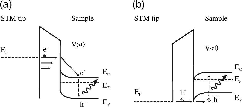 With the positive sample bias, the luminescence becomes observable after the bias voltage exceeds a threshold of , and it saturates around . The threshold voltage corresponds to the long-wavelength end of the spectra where the induced luminescence becomes observable. All of the peak positions remain constant for different excitation voltages. In the negative bias region, a weak emission is generated when the applied bias voltage surpasses , corresponding to the peak at around 619 nm in the spectra decomposition. The saturation is reached around , too. The observed luminescence intensity at negative bias is a few times lower than that at positive bias, which indicates that different generation-recombination processes of electron-hole pairs are responsible for the EL at opposite polarities. By applying the sample bias, which generates the flow of the tunneling current from the tip after it approached the p-type sample, electrons (in the case of positive bias), or holes (in the case of negative bias) are injected. The different luminescence processes can be explained with the energy diagram in Fig. 4: The Fermi level of the p-type sample (Er-doped silicon layer in our case) lies just above the valence band. At sufficient positive sample bias [Fig. 4(a)], the tunneling electrons (i.e., minority carriers) are injected into the conduction band, leading to direct recombination with majority carriers (i.e., holes) in the valence band and thereby to photon emission with energy equal to the band-gap energy.10 The increased number of emitted photons at lower temperatures (discussed below) also confirms such origin11: At low temperatures, major carriers (holes) are trapped in the acceptors and are capable of undergoing radiative recombination with free injected electrons. Under negative bias [Fig. 4(b)], hot holes injected from the tip have an impact ionization effect by which electron-hole pairs are excited, leading to the creation of extra electrons. These extra electrons then recombine radiatively with the majority carriers (holes) and relatively weak EL is emitted.12,13 To experimentally reveal the band gap of the structure, we used the STS technique for STM-induced electron emission measurement.14 The I-V curves are shown in Fig. 5(a). In the negative bias region, the bias threshold value is around ; in the positive bias region, the current starts being emitted at . The band gap for electron emission induced by electrons and holes is thus around 2.8 eV. Comparing the thresholds in Fig. 5(a) and 5(b) in the applied positive bias case, one can see an offset of about (). This offset cannot be sufficiently explained at present. Note that the observed band gap of the STM-induced photon emission is neither related to the band gap of , 8.8–9.8 eV as reported in Ref. 15, nor to that of , 7.6 eV as reported in Ref. 16. According to Ref. 17, corresponds to in . Calculating the direct band gap of at the corresponding temperature, with the binding energy of Er acceptors also taken into account, would enable us to estimate the radiation energies and compare them to the peak positions at EL spectrum. It would also be desirable to investigate the dependence of the STM-induced luminescence intensity as well as that of the PL intensity on the concentration of Er incorporated into the silicon material. Fig. 5I-V curve of the STM-induced electron emission. In the negative bias region, the bias threshold reaches a value of ; in the positive bias region, the current starts being emitted at , respectively. (b) Bias-dependence curve of the STM-induced photon emission with a constant current feedback of 800 nA. The threshold values at which the luminescence becomes observable are 1.2 V at positive bias and at negative bias, respectively.  Furthermore, to observe the change in radiation intensity and thereby validate the direct recombination process, we investigated the EL temperature dependence in the range from 80 to 293 K in the case of applied positive bias. The measurement revealed a few-fold increase in luminescence intensity with decreasing temperature; however, the shape of the spectrum was preserved. Because both the increase in the number of emitted photons and the sharpening of the peak shapes were observed with decreasing temperature, it could be deduced that the major carriers were frozen in impurities—acceptors (i.e., in Er).11 However, we could not determine whether the crystal field effect affects the splitting of energy levels, as 80 K was not low enough to reveal this effect. The lattice parameters and the elastic constants depend on temperature and magnetic field, the crystal-field excitation energies are modified, and these excitations are coupled to the phonons. The lowering of the symmetry by an applied external field introduces nonzero strains, proportional to the field, which change the symmetry of the lattice. The degeneracy of the ground state thus occurs, for example, because of hybridization of localized -electrons or the conduction electrons. The insufficiently low temperature thus causes damping of this splitting effect. We can evaluate the quantum efficiency of our sample according to the following equation: where is the luminescence intensity, is the photon detection efficiency of the optical detection system, is the tunneling current, and is the elementary charge. According to this equation, the quantum efficiency can be roughly estimated as .4.Conclusionwas deposited on by reactive magnetron sputtering and annealed at high temperature in Ar gas ambient. We found a region of ultrathin film on Si, where inner Er transitions become electrically active by applying both positive and negative bias; however, the emission at 1,535 nm is activated rarely. Significant regional dependence was also observed. The Er states in the oxide were determined. Additionally, the excitation spectrum was found to be continuous rather than to exhibit a single emission associated with the intra-4f transition: the main emissions are possibly related to the , , , , and transitions. The origin of the EL was reasonably explained by the radiative recombination of electron-hole pairs generated by electron injection in the case of positive sample bias, and by the radiative recombination of extra electrons, generated by impact ionization, with majority carriers in the case of negative sample bias. Determining the role of the structural-regional defects to elucidate the luminescence efficiency requires additional investigation together with time-resolved spectroscopy. AcknowledgmentsThe authors would like thank Dr. Toru Murashita for his insightful discussions. Jan Fiala is supported through a Vulcanus in Japan scholarship from the EU-Japan Center for Industrial Cooperation. ReferencesN. DaldossoL. Pavesi,
“Nanosilicon Photonics,”
Laser Photon. Rev., 3
(6), 508
–534
(2009). http://dx.doi.org/10.1002/lpor.v3:6 1863-8880 Google Scholar
A. J. Kenyonet al.,
“Optical properties of PECVD erbium-doped silicon-rich silica: evidence for energy transfer between silicon microclusters and erbium ions,”
J. Phys.: Condens. Matter, 6
(21), L319
–L324
(1994). http://dx.doi.org/10.1088/0953-8984/6/21/007 JCOMEL 0953-8984 Google Scholar
S. Scaleseet al.,
“Si:Er:O layers grown by molecular beam epitaxy: structural, electrical and optical properties,”
Mater. Sci. Eng. B, 81
(1–3), 62
–66
(2001). http://dx.doi.org/10.1016/S0921-5107(00)00728-5 MSBTEK 0921-5107 Google Scholar
O. Jamboiset al.,
“Towards population inversion of electrically pumped Er ions sensitized by Si nanoclusters,”
Opt. Express, 18
(3), 2230
–2235
(2010). http://dx.doi.org/10.1364/OE.18.002230 OPEXFF 1094-4087 Google Scholar
N. Daldossoet al.,
“Er-Coupled Si Nanocluster Waveguide,”
IEEE J. Sel. Top. Quant. Electron., 12
(6), 1607
–1617
(2006). http://dx.doi.org/10.1109/JSTQE.2006.885141 IJSQEN 1077-260X Google Scholar
C. A. BarriosM. Lipson,
“Electrically driven silicon resonant light emitting device based on slot-waveguide,”
Opt. Express, 13
(25), 10092
–10101
(2005). http://dx.doi.org/10.1364/OPEX.13.010092 OPEXFF 1094-4087 Google Scholar
I. Sychugovet al.,
“Modeling tip performance for combined STM-luminescence and aperture-SNOM scanning probe: Spatial resolution and collection efficiency,”
Appl. Surf. Sci., 254
(23), 7861
–7863
(2008). http://dx.doi.org/10.1016/j.apsusc.2008.03.005 ASUSEE 0169-4332 Google Scholar
I. Sychugovet al.,
“Optical and electrical characterization at the nanoscale with a transparent probe of a scanning tunneling microscope,”
Nanotechnology, 20
(14), 145706-1
–145706-4
(2009). http://dx.doi.org/10.1088/0957-4484/20/14/145706 NNOTER 0957-4484 Google Scholar
S. AbedrabboQ. MohammedA. T. Fiory,
“Processing for optically active erbium in silicon by film co-deposition and ion-beam mixing,”
Appl. Surf. Sci., 255
(8), 4503
–4511
(2009). http://dx.doi.org/10.1016/j.apsusc.2008.11.058 ASUSEE 0169-4332 Google Scholar
T. MurashitaK. Tateno,
“Direct measurement of sub-10 nm-level lateral distribution in tunneling-electron luminescence intensity on a cross-sectional 50-nm-thick AlAs layer by using a conductive transparent tip,”
Appl. Phys. Lett., 78
(25), 3995
–3997
(2001). http://dx.doi.org/10.1063/1.1380404 APPLAB 0003-6951 Google Scholar
P. Y. YuM. Cardona, Fundamentals of Semiconductors, 339 Springer, Berlin
(1996). Google Scholar
X. L. Guoet al.,
“Nanoscale electroluminesence from n-type GaAs(110) in tunnel junctions,”
Nanotechnology, 18
(19), 195201
(2007). http://dx.doi.org/10.1088/0957-4484/18/19/195201 NNOTER 0957-4484 Google Scholar
D. FujitaK. OnishiN. Niori,
“Light emission induced by tunneling electrons from a p-type GaAs(110) surface observed at near-field by a conductive optical fiber probe,”
Nanotechnology, 15
(6), S355
–S361
(2004). http://dx.doi.org/10.1088/0957-4484/15/6/E01 NNOTER 0957-4484 Google Scholar
C. C. UmbachJ. M. Blakely,
“Development of a sub-picoampere scanning tunneling microscope for oxide surfaces,”
Appl. Surf. Sci., 175–176 746
–752
(2001). http://dx.doi.org/10.1016/S0169-4332(01)00110-6 ASUSEE 0169-4332 Google Scholar
A. Janottiet al.,
“Interactions between nitrogen, hydrogen, and gallium vacancies in alloys,”
Phys. Rev. B, 67
(16), 161201-1
–161201-4
(2003). http://dx.doi.org/10.1103/PhysRevB.67.161201 PRBMDO 1098-0121 Google Scholar
Y. Y. Zhuet al.,
“Band offsets of films epitaxially grown on Si substrates,”
Appl. Phys. Lett., 88
(16), 162909-1
–162909-3
(2006). http://dx.doi.org/10.1063/1.2196476 APPLAB 0003-6951 Google Scholar
A. Barrancoet al.,
“Electronic state characterization of thin films prepared by evaporation,”
J. Appl. Phys., 97
(11), 113714-1
–113714-8
(2005). http://dx.doi.org/10.1063/1.1927278 JAPIAU 0021-8979 Google Scholar
Biography |


