|
|
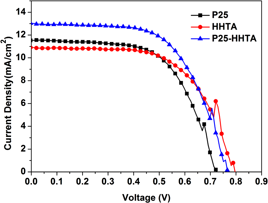
1.IntroductionDye-sensitized solar cells (DSCs) based on photosensitization of semiconductor materials have been studied extensively due to their relatively high efficiency, good stability, long life time, and low cost in materials and manufacturing.1–3 Photoelectrode is a key component of DSC devices, in which the processes of light absorption, charge generation, and electron collection take place.4 A typical DSC photoelectrode is made of mesoporous, wide band-gap semiconductor material deposited on a transparent conducting oxide (TCO) substrate. Oxide nanoparticles of 10 to 20 nm in diameter may provide a high specific surface area for dye adsorption and therefore have been widely used in DSCs to form the photoelectrode film. However, the thickness of a nanoparticle film is limited by the diffusion length of photoexcited electrons, which is usually more than 10 μm, and, as a result, the photoelectrode film comprised of nanoparticles alone usually cannot fulfill a complete light absorption.5,6 In other words, a portion of incident light may transmit through the nanoparticle film and makes no contribution to the electron-hole pair generation. For this reason, large particles (300 to 400 nm in diameter) acting as light scatterers have been used to combine with nanoparticles ( in diameter) to form the photoelectrode films with either a mixture structure or a bilayer structure.7–11 However, the use of large particles would inevitably result in a loss of internal surface area of the photoelectrode film.8,11 Recently, a new nanostructured material, a so-called aggregate, consisting of oxide nanocrystallites has been identified to be a promising material for high-efficiency DSCs, demonstrating the dual function of providing a high surface area for dye adsorption and generating efficient light scattering. In literature, it has been reported that the photoelectrode made of ZnO aggregates may achieved a power-conversion efficiency (PCE) of 5.4%, much higher than that of 2.4% for ZnO nanoparticles.12–14 aggregates have also demonstrated the capability to enhance the DSC performance compared with nanoparticles.15,16 However, the synthesis of nanocrystallite aggregates is still a challenge while considering that the enhancement of PCE by 15 to 30% is rather modest,15,17 due mainly to the difficulty in controlling the size and internal porosity of aggregates, which determine the light-scattering intensity and the penetration of dye molecules, respectively. Kim et al.17 reported that the size of internal pores in aggregates was around 10 nm, much smaller than the average pore size of 28.7 nm in a nanoparticle film. In addition to affecting the penetration of dye molecules, such a small internal pore size might also limit the diffusion of electrolyte while the solar cell is under the condition of operation. To receive a nanostructure that may, on one hand, retain the advantages of nanocrystallite aggregates in providing large surface area and the capability of light scattering and, on the other hand, overcome the insufficiency of the existing nanocrystallite aggregates reported so far with small internal pore size; in this paper we report a coaxial electrospray method for the fabrication of hollow hemispherical aggregates (HHTAs) consisting of nanocrystallites. The HHTAs possess a micrometer-sized hollow hemispherical structure responsible for light scattering, and the constitution of the HHTAs comprised of nanocrystallites may deliver desired specific surface area for sufficient adsorption of dye molecules for DSC application. In addition, compared with the hollow spheres reported elsewhere,18–20 the HHTAs have more open structure that allows more complete penetration of dye and more efficient diffusion of electrolyte. Although the advantages are listed above, the HHTAs show a drawback in providing relatively low surface area due to their unique hollow hemispherical structure. To solve this problem, in the present paper, the HHTAs used were combining with nanoparticles to form a bilayer photoelectrode that was composed of nanocrystallites at the bottom to provide large surface area for optical absorption and HHTAs at the top to function as light scatterers. The design of such a double-layer-structured photoelectrode film is also out of consideration to decrease the loss of incident light due to reflection by the HHTAs. This paper presents a systematical investigation of the relations between the structure of the photoelectrode film consisting of HHTAs and the power conversion efficiency, the charge transfer properties, and the diffusion reflectance. 2.ExperimentalCoaxial electrospray technique has been reported as a way to produce core-shell encapsulation for applications in areas such as food additives and targeted drug delivery.21–23 This technique was employed in our study for the synthesis of HHTAs by coaxial electrospraying two immiscible liquids for the formation of hollow hemispherical structure. The mechanism of immiscible liquids’ coaxial electrospray can be found elsewhere.24–26 Figure 1(a) is a schematic drawing of the coaxial electrospray system setup used in this study. The spray nozzle consists of two capillaries coaxially arranged with a 27-gauge inner needle and a 20-gauge outer needle. The capillary arrangement in the spray nozzle creates two separate liquid flow channels. Cooking oil (soybean oil, Kirkland SignatureTM) was used as the inner liquid; a colloidal dispersion containing P25 nanocrystallites was used as the outer liquid. The inner and outer liquids are injected into separate flow channels using two syringe pumps with different flow rates. A high-voltage power supply was employed to apply an electric field between the spray nozzle and the counter electrode. Fig. 1Schematic diagram illustrating: (a) the setup of the coaxial electrospray process for the formation of HHTAs and (b) the shell structure of the as-prepared HHTAs. 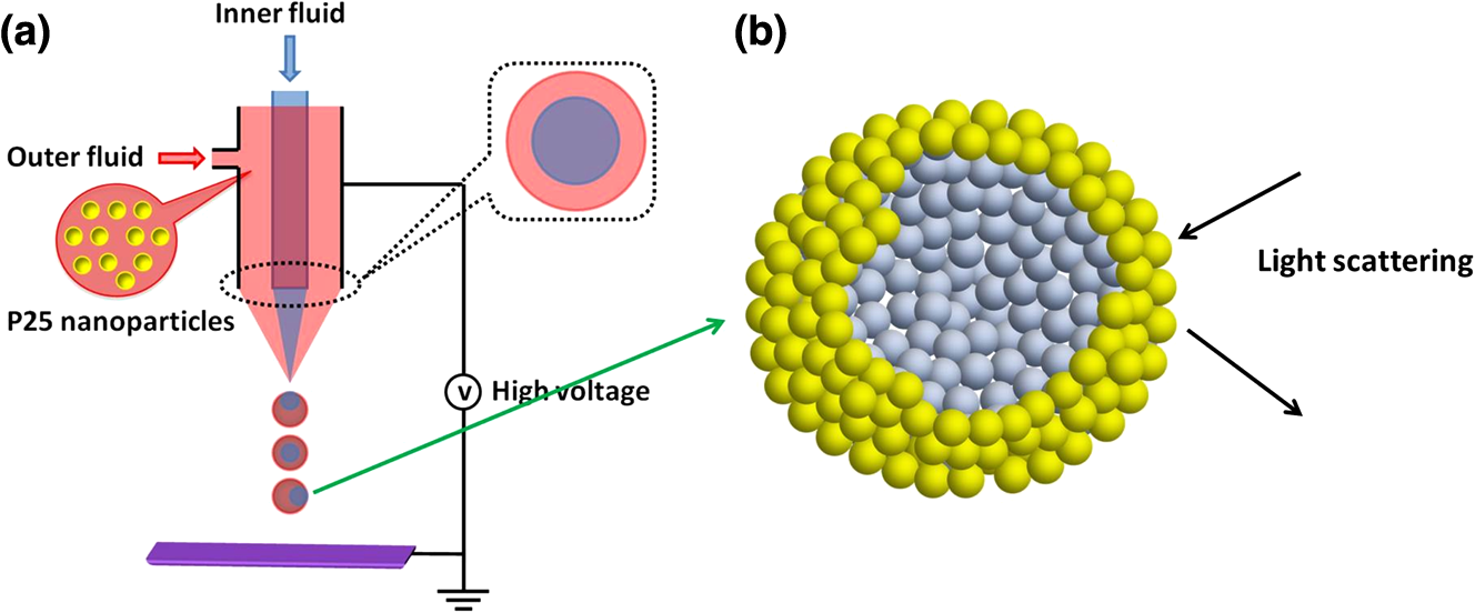 Figure 1(b) illustrates the shell structure of the as-prepared HHTAs. As the hollow spheres reported in literatures, which can enhance light harvesting efficiency and lead to a greatly improved photocatalytic activity or PCE,27–30 the HHTAs may also generate effective light scattering and enhance the optical abosorption of the photoelectrode film in view of their size comparable to the wavelengths of visible light. In a typical experiment for the synthesis of HHTAs through using the coaxial electrospray technique, 1 g P25 nanocrystallites (75% anatase and 25% rutile, Degussa) was dispersed in 10 ml of the mixed ethanol-water solvent (, ). After an ultrasonic treatment for 30 min, 0.1 g polyvinylpyrrolidone (PVP, ) was added and stirred vigorously until a homogeneous colloidal suspension was formed. PVP was used to adjust the viscosity of the suspension and create the porous structure of the HHTAs. The as-prepared suspension was water phase and used for electrospray as outer liquid. The inner liquid as oil phase was a cooking oil. These two immiscible liquids were loaded into two electrospray syringes and injected with flow rates of and for the outer liquid and the inner liquid, respectively. The distance from the nozzle to the counter electrode was 18 cm. The voltage applied to the coaxial spray nozzle and the counter electrode (i.e., the collecting substrate) was 24 kV. After the electrospray process, the resultant droplets were collected and dried at 80°C in air for further use. To make photoelectrode films, a paste was prepared by mixing the HHTAs with an organic vehicle based on -terpineol and ethyl cellulose. The paste was then deposited on fluorine-doped tin oxide (FTO) glass substrate to form a photoelectrode film via a doctor blading method. The films were then sintered at 150°C for 30 min and 500°C for 30 min in air. For comparison, photoelectrode films made of P25 nanocrystallites were also prepared with the same procedures. For the bilayer structure, a HHTA layer was fabricated on a P25 nanocrystallite film that was precalcined. The bilayer film was then sintered using the same sintering profile as that for the HHTAs and P25 layer, i.e., at 150°C for 30 min and 500°C for 30 min. The resulting films were sensitized with 0.5 mM ruthenium-based N3 dye solution for 24 h at room temperature. A platinum-coated silicon substrate as counter electrode was employed to set up the solar cell devices. The liquid electrolyte was composed of 0.6 M tetrabutylammonium iodide, 0.1 M lithium iodide, 0.1 M iodine, and 0.5 M 4-tert-butylpyridine in acetonitrile. Thermogravimetric analysis (TGA 7, Perkin-Elmer) was used to investigate the thermal behavior of HHTA photoelectrodes as a function of the annealing temperature. The morphology of HHTAs was characterized by field-emission scanning electron microscopy (FE-SEM, JEOL JSM-7000). X-ray diffraction (XRD, Philips PW 1830 Diffractometer) was employed to verify the phase of HHTAs. The adsorption amount of N3 dye on the photoelectrode films was studied by desorbing the dye from the photoelectrode film through a 0.1 M NaOH solution in water and ethanol (, ) and then measuring the optical absorption of the resultant solutions containing dye using an ultraviolet-visible-near-infrared spectrophotometer (UV-VIS-NIR, Perkin Elmer Lambda 900). The reflectance spectra of the photoelectrodes were obtained via an UV-VIS-NIR spectrometer equipped with integrating sphere. Photocurrent-voltage measurements were performed by recording the current-voltage data while the cells were irradiated by a simulated AM 1.5 light source with an output power density of . A Semiconductor Parameter Analyzer (4155A, Hewlett-Packard, Japan) was used to measure the current and voltage. The electrochemical impedance spectroscopy (EIS) was carried out through the Solartron 1287A coupling with the Solartron 1260 FRA/impedance analyzer to investigate electronic and ionic processes in DSCs. 3.Results and DiscussionFigure 2 shows the scanning electron microscopy (SEM) images of the HHTA film. It can be seen that the HHTA film is composed of polydisperse hollow hemispherical aggregates with diameters of 1 to 3 μm. The high-magnification SEM image in Fig. 2(b) reveals the hollow hemispherical structure of HHTAs consisting of P25 nanocrystallites. Figure 2(c) is a transmission electron microscopy (TEM) image of the individual HHTAs, which confirms the porous structure of HHTAs made of primary nanocrystallites in diameter. Shown in Fig. 2(d) is the TGA result of HHTA film composed of the resultant droplets from electrospray and the organic vehicle from the paste. It shows a very slight weight loss below 100°C and an weight loss at the temperatures ranging from 100°C to 225°C; the latter is ascribed to the decomposition of -terpineol in the paste in view of its boiling point of 212°C. More significant weight loss of more than 48% was found at the temperatures between 225°C and 460°C, suggesting the thermal decomposition and oxidation of organic compounds used in both the electrospray process and the paste preparation, for instance, PVP, ethyl cellulose, and cooking oil.31,32 No further weight loss was observed at temperatures higher than 460°C, indicating the complete removal of the organic components. The annealing temperature of HHTA film used in this study was accordingly set to 500°C to ensure a complete removal of the organic components. Note that, for comparison, the same annealing temperature was applied to P25 nanocrystallite film. The x-ray diffraction (XRD) patterns of the annealed HHTA and the P25 nanocrystallite films of the same thickness on FTO substrates are shown in Fig. 2(e). The patterns indicate the same crystal phase for both films, demonstrating that the coaxial electrospray fabrication and the consequent thermal treatment did not result in any detectable change in the phase structure of P25 nanocrystallites. It is worth noting that the intensity of anatase peak of P25 nanoparticle film is much higher than that of the HHTA film while the thicknesses of the films are the same. This suggests that, in the case of same thickness, the nanoparticle film possesses 34% more mass than the HHTA film due to a difference in the packing density. Fig. 2SEM images of (a) the as-synthesized HHTA film calcined at 500°C for 30 min; (b) high-magnification SEM image; (c) TEM image for individual HHTAs; (d) TGA result for as-synthesized HHTA film dried at 150°C for 30 min; (e) x-ray diffraction patterns of HHTA film and P25 nanocrystallite film of the same thickness on FTO substrates calcined at 500°C. The XRD peaks of FTO substrate are marked with asterisks. 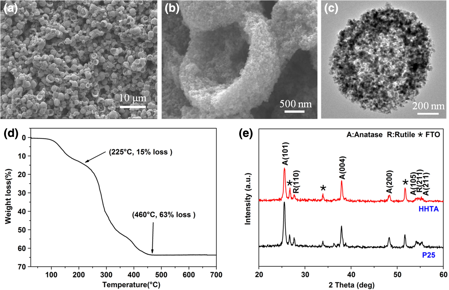 Three groups of photoelectrode films made of (1) P25 nanocrystallites (P25); (2) HHTAs (HHTA); and (3) bilayer structure with P25 nanocrystallite film on the bottom and an overlayer of HHTAs (P25-HHTA) were prepared and investigated their optical and photovoltaic properties. Figure 3 displays the cross-section SEM images of these films having the same thickness . The P25-HHTA bilayer photoelectrode was composed of 8.5-μm-thick P25 underlayer and 6.5-μm-thick HHTA overlayer. Fig. 3Cross-sectional SEM images of the photoelectrodes: (a) P25 nanocrystallites; (b) the P25-based bilayer structure having an overlayer of HHTAs (P25-HHTA); (c) HHTA. The scale bar is 10 μm. 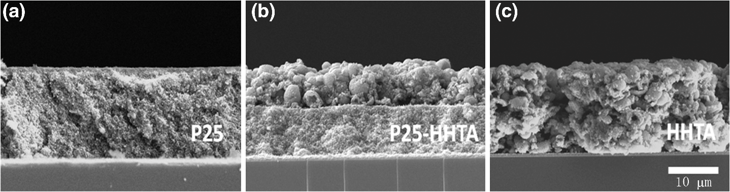 Figure 4 shows the UV-Vis diffuse reflectance spectra of all three photoelectrode films before and after dye-loading. From Fig. 4(a), it can be seen that all films before dye loading show intensive diffuse reflectance at the short wavelengths ranging from 400 and 500 nm. At wavelengths from 500 to 800 nm, the intensity of diffuse reflectance of HHTA films presents to decrease much more slowly than that of the film composed of P25 nanocrystallites. This can be explained by light scattering of HHTAs, which have more suitable structure for light scattering than the P25 nanocrystallites that also form agglomeration structure naturally. The P25-HHTA bilayer photoelectrode film consists of both P25 nanocrystallites and HHTA, and therefore the intensity of diffuse reflectance of it falls between those of the HHTA and P25 films. From Fig. 4(b), at long wavelengths (over 600 nm), the same trend was observed in comparison of the intensity of diffuse reflectance of these three photoelectrode films after dye loading, which confirms the high light-scattering capability of HHTAs. It is to be noted that the diffuse reflectance spectra of the three films after dye sensitization decreases drastically in the short wavelength region ranging from 400 to 600 nm, mainly due to light absorption by the N3 dye molecules.33 Fig. 4UV-Vis diffuse reflectance spectra of the photoelectrodes (a) before and (b) after dye-loading. 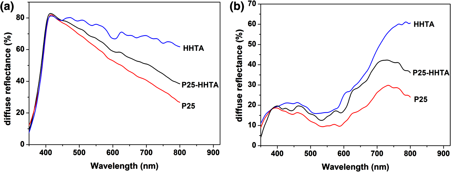 Figure 5 shows the typical I-V curves of the DSCs with P25, P25-HHTA and HHTA, respectively. The average open-circuit voltage (), short-circuit current density (), fill factor (FF), power conversion efficiency (PCE, ) of these solar cells are summarized in Table 1, which also includes the roughness factors defined as the total surface area per unit substrate area. In experiment, the roughness factor, , can be determined through the dye adsorption-desorption measurement34,35 and calculated by the following equation:34 where is the adsorbed amount of dye molecules (), is Avogadro’s number, and is the area occupied by one N3 dye molecule ().36 The was calculated by measuring the absorption spectra of the desorbed-dye solutions. According to experimental data and the Eq. (1), the roughness factor of P25 nanocrystallite photoelectrode was calculated to be 863, which was much higher than that of 533 for HHTA photoelectrode, indicating that the effective surface area for dye adsorption for nanocrystallite photoelectrode is larger than that for HHTA photoelectrode. This is in agreement with the XRD result mentioned above, which demonstrated the internal surface of P25 nanocrystallite film is 34% higher than that of HHTA film, while the film thickness is the same. For photoelectrode film, the larger surface area means more dye adsorption and more optical absorption. However, from the data shown Table 1, it can be seen that the nanocrystallite photoelectrode receives short-circuit current density of , compared with for HHTA electrode, indicating only enhancement. This result suggests that, although the HHTA photoelectrode film presents smaller surface area and less dye adsorption compared with P25 nanocrystallite film, it benefits from light scattering and therefore achieves photocurrent density as well as conversion efficiency close to that of P25 nanocrystallite film. The lower open-circuit voltage, , of the P25 DSCs while compared with that of for HHTA, is possibly due to larger surface area of nanocrystallite photoelectrode, which results in an increase of the charge recombination.8,33,37Table 1Comparison of the average open-circuit voltage (Voc), short-circuit current density (Jsc), fill factor (FF), power conversion efficiency (η), together with the roughness factors of the photoelectrodes based on P25, P25-HHTA, and HHTA.
The double-layered P25-HHTA structure was purposely designed to overcome the disadvantage of HHTA film in surface area and lower the back-scattering of the HHTAs to the incident light. The roughness factor of P25-HHTA photoelectrode increases to 657 as compared to 533 for HHTA photoelectrode, well indicating an increase in the surface area of photoelectrode due to the integration of HHTA film with P25 nanocrystallite film. The average conversion efficiency of the solar cell with P25-HHTA photoelectrode, , is appreciably higher than those of for P25 and for HHTA, when other device parameters were kept the same. The achievement of the highest efficiency for P25-HHTA can be attributed to the combination of effective light scattering generated by the HHTA overlayer and large surface area provided by the P25 nanocrystallite underlayer. The following discussion will further demonstrate that the use of HHTA overlayer may decrease the number of boundaries compared with the case of single layer film with nanoparticles alone and therefore lead to less recombination and higher open-circuit voltage. EIS was employed to study the charge transfer properties in the DSCs. The measurement was carried out under open-circuit condition and frequencies ranging from 0.05 Hz to 100 kHz. Figure 6(a) shows the typical EIS Nyquist plots of the DSCs with P25, P25-HHTA, and HHTA, respectively. The results reveal that all spectra are composed of two semicircles with a small one in the high-frequency region and a large one in the low-frequency region. An equivalent circuit as given in Fig. 6(b) was adopted to fit the EIS data: the small semicircle represents the charge transfer resistance () corresponding with the charge transfer process occurring at the interface between the counter electrode and the electrolyte containing redox couple . The large semicircle originates from the charge transport resistance () related to the electron transport process within the films and the charge transfer process at the interfaces between the and the electrolyte/dye.38–40 , shown in the equivalent circuit, represents the series ohmic resistance existing in the external circuit. CPEs are constant phase elements resulting from the capacitor components in the solar cell. The , , and values fitted to the equivalent circuit are listed in Table 2. Interestingly, the charge transport resistances () of P25, HHTA, and P25-HHTA photoelectrodes increase in the order . The highest charge transport resistance () of the HHTA photoelectrode is a result of point-contact among the spherical HHTAs, which possess micron meter size and give rise to interconnection poorer than the case of nanocrystallite photoelectrode. However, the highest received by the HHTA photoelectrode in turn implies that the electron transport within the HHTAs is highly efficient and accordingly can effectively compensate the increased recombination in the HHTA photoelectrode represented by the larger transport resistance. This is in agreement with the findings in literature emphasizing that the nanocrystallite aggregates or mesoporous beads having a closely packed structure may better conduct the electron transport than dispersed nanoparticles.41,42 Fig. 6(a) EIS spectroscopy for the DSCs with the photoelectrodes of P25, P25-HHTA, and HHTA. (b) The fitted equivalent circuit. 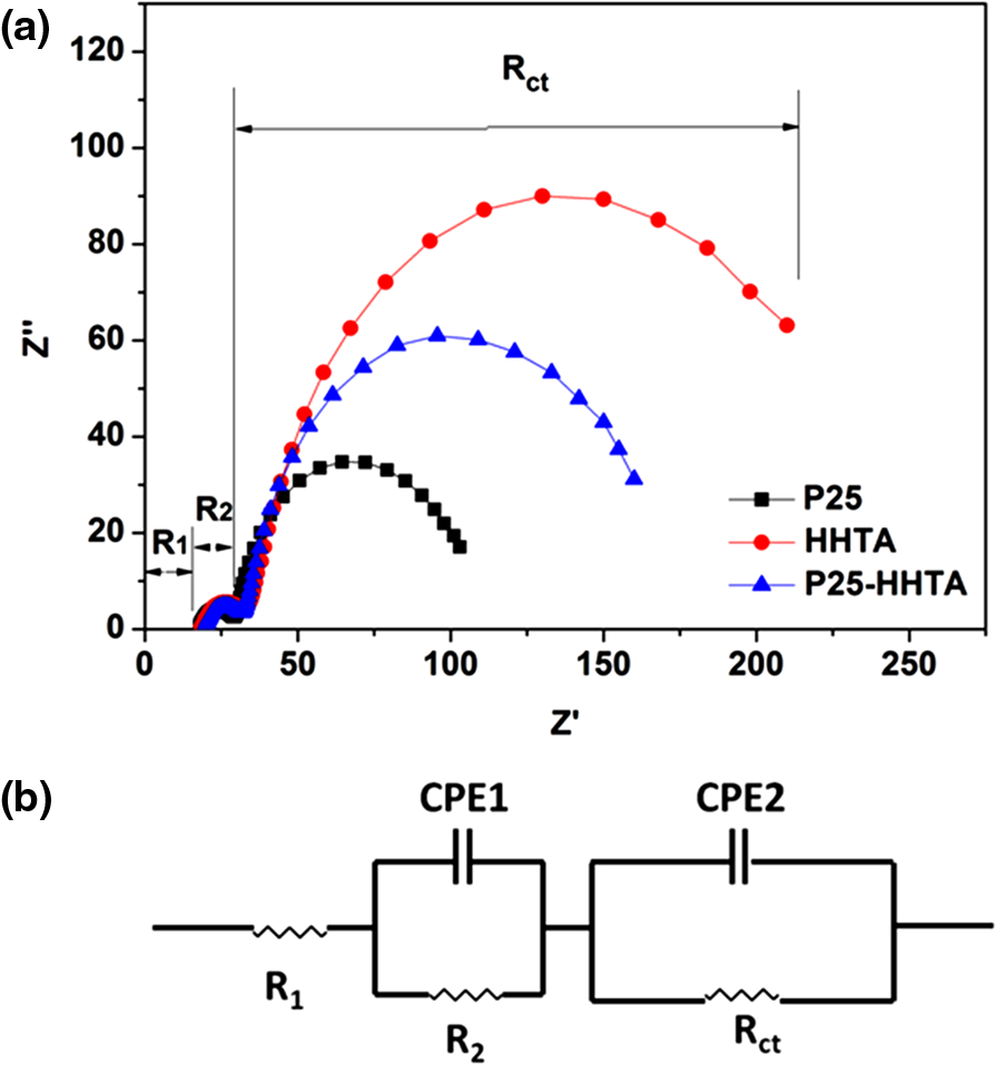 Table 2Summary of EIS results obtained by fitting the impedance spectra of DSCs with the photoelectrodes of P25, P25-HHTA, and HHTA using the equivalent circuit in Fig. 6(b).
4.ConclusionMicrometer-sized hollow hemispherical aggregates (HHTAs) made of primary P25 nanocrystallites were successfully fabricated by means of the coaxial electrospray method. The coaxial electrospray did not cause any detectable change in the crystallinity or phases of the P25 nanocrystallites and therefore the merit of nanocrystallites in the facets for dye adsorption could be well remained. The average conversion efficiency of 6.05%–0.5% obtained for bilayer photoelectrode with the P25 nanocrystallites as underlayer and the HHTAs as scattering overlayer was higher than the values of and for P25 and HHTA photoelectrodes, respectively. The advantage of the HHTAs for DSC application can be summarized to the following aspects: 1. the HHTAs with size comparable to the wavelengths of visible light can generate effective light scattering; 2. the constitution of the HHTAs with nanocrystallites may ensure a large surface area for dye adsorption; and 3. the closely packed structure of nanocrystallites within the HHTAs enables a highly efficient electron transport that can significantly reduce the charge recombination in the DSCs. AcknowledgmentsJ.T.X. gratefully acknowledges the fellowship from China Scholarship Council. This work has been supported in part by National Natural Science Foundation of China (21173042), Natural Science Foundation of Jiangsu Province (BK2011589), the US Department of Energy, Office of Basic Energy Sciences, Division of Materials and Engineering under Award No. DE-FG02-07ER46467 (Q.F.Z.), National Science Foundation (DMR-1035196), Boeing-Steiner Endowment, University of Washington TGIF grant and Intel Corporation. In this research work, all co-authors have made significant contributions. J.X. fabricated the hollow hemispherical aggregates and applied them to DSCs. J.X. measured most of the properties of both materials and solar cells. Q.Z. and D.M. characterized the microstructure properties and measured power conversion efficiency. Y.S. and G.Z. were responsible for the overall scope and conduct of the reported research. ReferencesB. OreganM. Gratzel,
“A low-cost, high-efficiency solar cell based on dye-sensitized colloidal films,”
Nature, 353 737
–740
(1991). http://dx.doi.org/10.1038/353737a0 NATUAS 0028-0836 Google Scholar
Q. F. ZhangG. Z. Cao,
“Nanostructured photoelectrodes for dye-sensitized solar cells,”
Nano Today, 6
(1), 91
–109
(2011). http://dx.doi.org/10.1016/j.nantod.2010.12.007 1748-0132 Google Scholar
Q. F. Zhanget al.,
“ZnO Nanostructures for dye-sensitized solar cells,”
Adv. Mater., 21
(41), 4087
–4108
(2009). http://dx.doi.org/10.1002/adma.v21:41 ADVMEW 0935-9648 Google Scholar
J. Y. Zhanget al.,
“Ligand-assisted assembly approach to synthesize large-pore ordered mesoporous titania with thermally stable and crystalline framework,”
Adv. Energy Mater., 1
(2), 241
–248
(2011). http://dx.doi.org/10.1002/aenm.201000004 Google Scholar
H. M. Zhanget al.,
“Anatase microspheres with exposed mirror-like plane {001} facets for high performance dye-sensitized solar cells (DSSCs),”
Chem. Commun., 46
(44), 8395
–8397
(2010). http://dx.doi.org/10.1039/c0cc03196h CHCOFS 1364-548X Google Scholar
L. I. HalaouiN. M. AbramsT. E. Mallouk,
“Increasing the conversion efficiency of dye-sensitized photoelectrochemical cells by coupling to photonic crystals,”
J. Phys. Chem. B, 109
(13), 6334
–6342
(2005). http://dx.doi.org/10.1021/jp044228a JPCBFK 1520-6106 Google Scholar
J. FerberJ. Luther,
“Computer simulations of light scattering and absorption in dye-sensitized solar cells,”
Sol. Energy Mater. Sol. Cells, 54
(1–4), 265
–275
(1998). http://dx.doi.org/10.1016/S0927-0248(98)00078-6 SEMCEQ 0927-0248 Google Scholar
Z. S. Wanget al.,
“Significant influence of photoelectrode morphology on the energy conversion efficiency of N719 dye-sensitized solar cell,”
Coord. Chem. Rev., 248
(13–14), 1381
–1389
(2004). http://dx.doi.org/10.1016/j.ccr.2004.03.006 CCHRAM 0010-8545 Google Scholar
S. Itoet al.,
“Fabrication of thin film dye sensitized solar cells with solar to electric power conversion efficiency over 10%,”
Thin Solid Films, 516
(14), 4613
–4619
(2008). http://dx.doi.org/10.1016/j.tsf.2007.05.090 THSFAP 0040-6090 Google Scholar
A. Usami,
“Theoretical study of application of multiple scattering of light to a dye-sensitized nanocrystalline photoelectrochemical cell,”
Chem. Phys. Lett., 277
(1–3), 105
–108
(1997). http://dx.doi.org/10.1016/S0009-2614(97)00878-6 CHPLBC 0009-2614 Google Scholar
J. T. Xiet al.,
“Enhanced power conversion efficiency in dye-sensitized solar cells with aggregates/nanocrystallites mixed photoelectrodes,”
Electrochim. Acta, 56
(5), 1960
–1966
(2011). http://dx.doi.org/10.1016/j.electacta.2010.11.054 ELCAAV 0013-4686 Google Scholar
T. P. Chouet al.,
“Hierarchically structured ZnO film for dye-sensitized solar cells with enhanced energy conversion efficiency,”
Adv. Mater., 19
(18), 2588
–2592
(2007). http://dx.doi.org/10.1002/(ISSN)1521-4095 ADVMEW 0935-9648 Google Scholar
K. Parket al.,
“Effect of an ultrathin layer coated on submicrometer-sized ZnO nanocrystallite aggregates by atomic layer deposition on the performance of dye-sensitized solar cells,”
Adv. Mater., 22
(21), 2329
–2332
(2010). http://dx.doi.org/10.1002/adma.200903219 ADVMEW 0935-9648 Google Scholar
Q. F. Zhanget al.,
“Aggregation of ZnO nanocrystallites for high conversion efficiency in dye-sensitized solar cells,”
Angew. Chem.-Int. Edit., 47
(13), 2402
–2406
(2008). http://dx.doi.org/10.1002/(ISSN)1521-3773 1433-7851 Google Scholar
D. H. Chenet al.,
“Mesoporous anatase beads with high surface areas and controllable pore sizes: a superior candidate for high-performance dye-sensitized solar cells,”
Adv. Mater., 21
(21), 2206
–2210
(2009). http://dx.doi.org/10.1002/adma.v21:21 ADVMEW 0935-9648 Google Scholar
W. Shaoet al.,
“Interfacial confined formation of mesoporous spherical nanostructures with improved photoelectric conversion efficiency,”
Inorg. Chem., 49
(12), 5453
–5459
(2010). http://dx.doi.org/10.1021/ic902553f INOCAJ 0020-1669 Google Scholar
Y. J. Kimet al.,
“Formation of highly efficient dye-sensitized solar cells by hierarchical pore generation with nanoporous spheres,”
Adv. Mater., 21
(36), 3668
–3673
(2009). http://dx.doi.org/10.1002/adma.v21:36 ADVMEW 0935-9648 Google Scholar
J. F. Qianet al.,
“-coated multilayered hollow microspheres for dye-sensitized solar cells,”
Adv. Mater., 21
(36), 3663
–3667
(2009). http://dx.doi.org/10.1002/adma.v21:36 ADVMEW 0935-9648 Google Scholar
G. T. Daiet al.,
“A novel photoanode architecture of dye-sensitized solar cells based on TiO(2) hollow sphere/nanorod array double-layer film,”
J. Colloid Interface Sci., 365
(1), 46
–52
(2012). http://dx.doi.org/10.1016/j.jcis.2011.08.073 JCISA5 0021-9797 Google Scholar
M. Chiganeet al.,
“Preparation of hollow titanium dioxide shell thin films by electrophoresis and electrolysis for dye-sensitized solar cells,”
Electrochem. Solid-State Lett., 12
(5), E5
–E8
(2009). http://dx.doi.org/10.1149/1.3089877 ESLEF6 1099-0062 Google Scholar
Y. J. Jinget al.,
“Ultrasound-triggered smart drug release from multifunctional core-shell capsules one-step fabricated by coaxial electrospray method,”
Langmuir, 27
(3), 1175
–1180
(2011). http://dx.doi.org/10.1021/la1042734 LANGD5 0743-7463 Google Scholar
H. Y. Chenet al.,
“One-step multicomponent encapsulation by compound-fluidic electrospray,”
J. Am. Chem. Soc., 130
(25), 7800
–7801
(2008). http://dx.doi.org/10.1021/ja801803x JACSAT 0002-7863 Google Scholar
F. MeiD. R. Chen,
“Investigation of compound jet electrospray: Particle encapsulation,”
Phys. Fluids, 19
(10), 103303
(2007). http://dx.doi.org/10.1063/1.2775976 PHFLE6 1070-6631 Google Scholar
A. G. Marinet al.,
“Simple and double emulsions via coaxial jet electrosprays,”
Phys. Rev. Lett., 98
(1), 014502
(2007). http://dx.doi.org/10.1103/PhysRevLett.98.014502 PRLTAO 0031-9007 Google Scholar
Z. Ahmadet al.,
“Engineering a material for biomedical applications with electric field assisted processing,”
Appl. Phys. A-Mater. Sci. Process., 97
(1), 31
–37
(2009). http://dx.doi.org/10.1007/s00339-009-5359-z 0947-8396 Google Scholar
X. P. Chenet al.,
“Spraying modes in coaxial jet electrospray with outer driving liquid,”
Phys. Fluids, 17
(3), 032101
(2005). http://dx.doi.org/10.1063/1.1850691 PHFLE6 1070-6631 Google Scholar
X. X. Liet al.,
“Large-scale fabrication of hierarchical hollow spheres,”
Inorg. Chem., 45
(9), 3493
–3495
(2006). http://dx.doi.org/10.1021/ic0602502 INOCAJ 0020-1669 Google Scholar
H. X. Liet al.,
“Mesoporous titania spheres with tunable chamber structure and enhanced photocatalytic activity,”
J. Am. Chem. Soc., 129
(27), 8406
–8407
(2007). http://dx.doi.org/10.1021/ja072191c JACSAT 0002-7863 Google Scholar
H. J. Kooet al.,
“Nano-embossed hollow spherical as bifunctional material for high-efficiency dye-sensitized solar cells,”
Adv. Mater., 20
(1), 195
–199
(2008). http://dx.doi.org/10.1002/(ISSN)1521-4095 ADVMEW 0935-9648 Google Scholar
Y. W. Zhanget al.,
“Anatase hollow spheres embedded nanocrystalline photoanode for dye-sensitized solar cells,”
Mater. Chem. Phys., 123
(2–3), 595
–600
(2010). http://dx.doi.org/10.1016/j.matchemphys.2010.05.020 MCHPDR 0254-0584 Google Scholar
R. Moriet al.,
“Organic solvent based dispersion paste for dye-sensitized solar cells prepared by industrial production level procedure,”
J. Mater. Sci., 46
(5), 1341
–1350
(2011). http://dx.doi.org/10.1007/s10853-010-4925-2 JMTSAS 0022-2461 Google Scholar
M. Nedelcuet al.,
“Monolithic route to efficient dye-sensitized solar cells employing diblock copolymers for mesoporous ,”
J. Mater. Chem., 20
(7), 1261
–1268
(2010). http://dx.doi.org/10.1039/b920077k JMACEP 0959-9428 Google Scholar
C. X. Heet al.,
“Sonochemical preparation of hierarchical ZnO hollow spheres for efficient dye-sensitized solar cells,”
Chem. Eur. J., 16
(29), 8757
–8761
(2010). http://dx.doi.org/10.1002/chem.201000264 CEUJED 0947-6539 Google Scholar
C. Y. Yenet al.,
“Preparation and properties of a carbon nanotube-based nanocomposite photoanode for dye-sensitized solar cells,”
Nanotechnology, 19
(37), 375305
(2008). http://dx.doi.org/10.1088/0957-4484/19/37/375305 NNOTER 0957-4484 Google Scholar
G. Kantoniset al.,
“Electron dynamics dependence on optimum dye loading for an efficient dye-sensitized solar cell,”
J. Photochem. Photobiol. A:Chemistry, 217
(1), 236
–241
(2011). http://dx.doi.org/10.1016/j.jphotochem.2010.10.015 1010-6030 Google Scholar
A. HagfeldtM. Gratzel,
“Molecular photovoltaics,”
Acc. Chem. Res., 33
(5), 269
–277
(2000). http://dx.doi.org/10.1021/ar980112j ACHRE4 0001-4842 Google Scholar
D. B. Kuanget al.,
“High molar extinction coefficient heteroleptic ruthenium complexes for thin film dye-sensitized solar cells,”
J. Am. Chem. Soc., 128
(12), 4146
–4154
(2006). http://dx.doi.org/10.1021/ja058540p JACSAT 0002-7863 Google Scholar
K. Parket al.,
“Charge transport properties of ZnO nanorod aggregate photoelectrodes for DSCs,”
J. Phys. Chem. C, 115
(43), 20992
–20999
(2011). http://dx.doi.org/10.1021/jp2067292 1932-7447 Google Scholar
F. Fabregat-Santiagoet al.,
“The origin of slow electron recombination processes in dye-sensitized solar cells with alumina barrier coatings,”
J. Appl. Phys., 96
(11), 6903
–6907
(2004). http://dx.doi.org/10.1063/1.1812588 JAPIAU 0021-8979 Google Scholar
F. Fabregat-Santiagoet al.,
“Influence of electrolyte in transport and recombination in dye-sensitized solar cells studied by impedance spectroscopy,”
Sol. Energy Mater. Sol. Cells, 87
(1–4), 117
–131
(2005). http://dx.doi.org/10.1016/j.solmat.2004.07.017 SEMCEQ 0927-0248 Google Scholar
K. Zhuet al.,
“Influence of surface area on charge transport and recombination in dye-sensitized solar cells,”
J. Phys. Chem. B, 110
(50), 25174
–25180
(2006). http://dx.doi.org/10.1021/jp065284+ JPCBFK 1520-6106 Google Scholar
X. A. Panet al.,
“ nanotubes infiltrated with nanoparticles for dye sensitized solar cells,”
Nanotechnology, 22
(23), 235402
(2011). http://dx.doi.org/10.1088/0957-4484/22/23/235402 NNOTER 0957-4484 Google Scholar
Biography Junting Xi received her BS in chemistry and chemical engineering from Southeast University in 2007. She is currently a PhD candidate in School of Chemistry and Chemical Engineering at Southeast University. She had been a visiting student at University of Washington for two years. Her current research is focused on the fabrication of semiconductor nanomaterials and their applications in photovoltaic devices.  Qifeng Zhang earned his PhD from Peking University. Currently he is research assistant professor in the Department of Materials Science and Engineering at University of Washington. His research interests involve engineering nano-structured materials for applications to electrical devices, including solar cells, UV light-emitting diodes (LEDs), field-effect transistors (FETs), and gas sensors. His current research is focused on dye-sensitized solar cells (DSCs), (CZTS)-based thin film solar cells, quantum dot solar cells, and organic/inorganic hybrid solar cells.  Daniel Myers earned his BS physics degree from the University of North Carolina at Chapel Hill and is currently a master’s degree student in mechanical engineering at the University of Washington. His research focus is on the optimization of the structure of dye-sensitized solar cells. He has also developed assembly methods for electrochromic windows.  Yueming Sun is currently the professor in School of Chemistry and Chemical Engineering at Southeast University. He received his PhD from Nanjing University. His research interests include molecular design of materials, theoretical and computational chemistry, design and fabrication of novel electrodes for applications in dye-sensitized solar cells and fuel cells.  Guozhong Cao is Boeing-Steiner professor of materials science and engineering, professor of chemical engineering, and adjunct professor of mechanical engineering at University of Washington. He received his PhD from Eindhoven University of Technology, MS from Shanghai Institute of Ceramics of Chinese Academy of Sciences, and BS from East China University of Science and Technology. His current research is focused mainly on chemical processing of nanomaterials for energy-related applications including solar cells, lithium-ion batteries, supercapacitors, and hydrogen storage. |