
|
|
1.IntroductionOver the last decade, many research efforts have been focused on the development of fast, sensitive, and low cost ways of detection, especially for biologic or chemical compounds. Three of them are principally chosen for such purpose: the enzyme-linked immunosorbent assay (ELISA) method,1 the quartz crystal microbalance device,2 and the surface waves based detections. In the first method, an unknown protein or antigen is first bound to a functionalized surface. It then interacts with an antibody labeled with a fluorophore in order to produce a detectable signal. Such method regularly succeeds in the detection of analyte concentration at the nanomolar order. However, ELISA is by definition a method that needs a label for detection and, therefore, it can induce modifications of the probe molecules. The quartz crystal microbalance exploits the change in frequency of a quartz crystal resonator to detect the binding of an analyte to an electrode surface. The limit of detection used by such device can be as low as the nanomolar.3 The third main way of detection based on surface waves uses the sensitivity of metallic component [flat layer for Surface Plasmon Resonance sensors or nanoparticles for Localized Surface Plasmon Resonance (LSPR) sensors] to any change in the surrounding medium. Under an excitation in the visible range, metallic nanoparticles (MNPs) have specific optical properties enabling the creation of a large electromagnetic near field around them. An enhancement of any optical information (scattering, emission) is therefore expected when an analyte is located at the vicinity of these nanoparticles. Whatever the sensors presented in this review, they are all based on the field enhancement at the nanoparticle vicinity provided by the localized surface plasmons (LSP). This field enhancement can be exploited in different manners for the detection or identification of an analyte being at the close vicinity of the nanoparticle surface. First, the information provided by the spectral shift of the LSP resonance can be directly exploited when an analyte is deposited on the nanoparticles surface (LSPR sensor). Second, other sensors are based on a light-matter interaction process such as fluorescence, Raman scattering or infrared absorption, which will benefit from the local electromagnetic field enhancement provided by LSP. They, respectively, give rise to metal enhanced fluorescence (MEF), surface enhanced Raman scattering (SERS), and surface enhanced infrared absorption (SEIRA) sensors. The high sensitivity provided by the near field enhancement enables the detection of small quantities of analyte. Two important advantages provided by nanosensors based on LSPR, SERS, and SEIRA is that unlike ELISA or MEF, they are label-free techniques and, since the size of the metallic particles is in the nanometer range, they open a way for sensor miniaturization. However, the strength of the electromagnetic near field depends on the geometrical parameters of the MNP for which nanolithographied techniques show a very precise control. This review is devoted to the description of sensors based on nanolithographied substrates. A description of the electromagnetic near field enhancement by MNPs is first given and followed by a description of the main nanolithographied techniques used to create nanosensors. An overview of nanosensors based on LSPR, SERS, and MEF is then provided. For each of these techniques, a presentation of the physical principle is given followed by the main applications. 2.Electromagnetic Enhancement by Metallic NanostructuresThe high sensitivity provided by the nanosensors described in this review is based on the electromagnetic field enhancement provided by MNPs. In this part, the origin of this enhancement is presented and the main parameters governing this enhancement are highlighted. The specificity of metallic materials is that their conduction electrons are weakly linked to the atoms nucleus. These electrons are therefore easy to move from their equilibrium position by providing either thermal or light energy. The optical response of a material under an incident electromagnetic field is described by the metal relative permittivity . In a metal, the incident field energy is dissipated by Joule effect and by the creation of a current density within the material, which is proportional to the incident electric field and to the metal conductivity known as the damping effect. The introduction of in the curl of the magnetic field of Maxwell’s equations and the application of the harmonic solutions of the electric field induce a change of the relative permittivity now expressed as:4 With , the plasma frequency; , the angular frequency of the excitation field; , the eigen frequency of the charges oscillations damping in the material; , a reduced constant in which dimension is an angular frequency linked to the viscous friction of the electric charges in the material; , the vacuum permittivity; and , the complex refractive index such as . The imaginary part of describes the absorption properties of the metallic material and means that the incident light intensity will decay inside the metal on a length called skin depth expressed as:4 With the material conductivity; the angular frequency of the excitation field; and the vacuum permeability.When considering a MNP, its size becomes comparable to the skin depth one. As a consequence, all the conductive electrons can interact with the incident electromagnetic field. The energy absorbed by the nanoparticle enables the electrons oscillations, which become collective due to Coulomb interaction at the nanoparticle scale. This phenomenon is called LSP, it is in resonance (LSPR) when its oscillation energy matches the incident field energy. The light interacting with the LSP can be absorbed or scattered by the nanoparticle. In the case of a spherical nanoparticle, the scattering, the absorption as well as the extinction () yields can be predicted by the classical Mie theory,5 which provides the exact solution of the Maxwell’s equations. The extinction spectrum maximum is then characteristic of the LSPR and corresponds to a particular wavelength. Mie’s theory can be simplified by considering a nanoparticle whose size is extremely small compared to the incident wavelength, i.e., 20 nm for silver and 40 nm for gold nanoparticle. In fact, this case corresponds to the quasistatic approximation (QSA) or dipolar approximation and is adapted to predict the resonance conditions, which corresponds to a maximum of the nanoparticle polarizability . In the particular case of a sphere embedded in a surrounding medium with a permittivity , is written as:6 When the imaginary part of the dielectric constant is small, is reached for . Thus, the permittivity of the surrounding medium (and the corresponding refractive index ) plays a key role in the determination of the resonance conditions since it controls the associated value of the real part of the effective relative permittivity of the metal. As a consequence, an increase of the refractive index surrounding the MNP leads to a decrease of . The maximum of the nanoparticle polarizability is therefore increased leading to a redshift of the LSPR wavelength.7 This is due to the accumulation of charges in the dielectric side that induces a damping of the total collective oscillation. When the resonance condition is reached, the electromagnetic field created at the vicinity of the nanosphere surface is enhanced. This is the key phenomenon on which the surface enhanced nanosensors considered in this review are based. This external local field is strongly sensitive to any changes in the metallic surface environment (e.g., solvent, molecule).In the case of spheroid shapes with three semi-axis , , and ; each axis has its own polarizability such as:8 with the geometrical factor of the nanoparticle ( for a sphere).As shown in the Fig. 1, if we consider one geometrical axis (with ), a spheroid flattened along the axis (oblate) leads to an increase of above . It induces a blueshift of the LSPR wavelength along the axis . On the opposite, a cigar-like spheroid (prolate) along the axis leads to a decrease of below . It induces a fast redshift of the LSPR wavelength. Fig. 1Evolution of the real part of versus the depolarization factor with examples of consequence on the ellipsoids shape in air ().  More generally, for a non spherical nanoparticle, the extinction spectrum exhibits three distinct maxima corresponding to the three LSPR excited in the three dimensions of the ellipsoid. The most redshifted one is then assigned to the LSPR along the longest axis, whereas the most blueshifted one is assigned to the LSPR along the shortest axis. The shape is therefore an important parameter to control the optical properties of such MNPs. The simple models just presented are very simple models enabling the extraction of key parameters that govern the resonance conditions. In order to simulate more complex nanoparticles and to approach the experimental conditions, complex models using the finite-difference time-domain method (FDTD), the discrete dipole approximation (DDA) and de finite-element method (FEM) are often used. When considering larger nanoparticles (typically above 40 nm for gold), the QSA has to be corrected since the nanoparticle size is no more negligible compared to the incident wavelength. As a consequence, (i) the conductive electrons do not oscillate exactly in phase all along the nanoparticle and leads to a decrease of the depolarization field (known as the retardation effect proportional to the square of the nanoparticle size9) and, (ii) the contribution of losses by radiation (radiation damping) is no more negligible and is proportional to the third power of the nanoparticle size.10 These two phenomena result, respectively, in a redshift and a broadening of the LSPR wavelength when the size of the metallic nanosphere increases. They are considered as first corrections of the QSA. Hence, the size of the MNP is a second key parameter that governs the resonance condition. If more than one MNP is considered, like an array for example, two kinds of dipolar interactions can modify the optical properties. If the interparticle gap is on the order of the incident wavelength, far-field dipolar interactions dominate and the coupling shows a dependence. These interactions shift the LSPR position and change the shape of the LSP.11 If is very small compared to the incident wavelength, near-field dipolar coupling dominates with a dependence of . This latter case has an important interest for sensing purpose since small gaps between MNPs can lead to areas with highly confined electromagnetic field,12,13 i.e., the so-called hot-spots. A decrease of the gaps between nanoparticles leads to a typical redshift of the LSPR position for an incident field polarization set along the coupling axis, while a blueshift is observed for a perpendicular polarization. It happens in whatever the chosen geometry of the nanoparticles is (e.g.. dimers,13–15 trimers,16 or chains17). Moreover, for polarization along the coupling axis, the coupling efficiency (defined as the ratio of the LSPR position shift between the interacting and non interacting case over the LSPR position of the non interacting case) increases exponentially as the ratio between and the nanoparticle size decreases.18,19 The choice of the metal is also an important point since the real and imaginary dielectric constant changes from one metal to another. Many types of MNPs such as Pd, Pt, Al, Au, and Ag exhibit plasmons. However, Au and Ag are the most chosen since they show highly intense LSPR in the visible range.20 Due to a lower imaginary part of for Ag (thus, lower losses), Ag nanoparticles provide a stronger electric near field and a sharper plasmon band than equivalent Au nanoparticles, and Ag is therefore more sensitive to the surrounding environment.21 However, Au nanoparticles are more often used in biological application purposes because they are considered as biocompatible material and tend to be more stable than Ag.21 In brief, the main parameters governing the optical properties of MNPs are the surrounding medium, the size, the shape, near or far field coupling and the material. It is thus easily understandable that a high control of the geometrical parameters is necessary when developing or optimizing sensors based on surface enhancement. The next part of this review is devoted to the fabrication techniques that demonstrated their ability to reach such purposes. 3.Surface Nanostructuration by Lithography TechniquesIn order to optimize the performance of a nanosensor with a LSPR position located in the visible range, arrays of gold nanoparticles have to be produced with a size below 200 nm (dipolar case). The nanoparticles geometrical parameters have to be highly controlled to investigate their efficiency for sensor application. The production techniques have to be highly reproducible to develop reliable sensor. The fulfillment of these two requirements is completed by the nanolithography techniques. These techniques provide excellent control of the nanoparticles size, shape and surface distribution and, therefore, of their optical properties. A large range of nanolithography techniques can be employed using top-down or bottom-up approaches. In this review, we distinguish conventional and unconventional nanolithographied techniques. For the first ones, we will focus on techniques based on either light transmission through a mask process (optical lithography) or on a focused beam process (electron and ion beam lithographies). In a second par, we will consider unconventional techniques, that is to say: substrates made by soft methods (nanoimprint lithography) as well as those that require a self-organization step (nanosphere lithography) will be described. 3.1.Conventional NanolithographiesThe main parameter that motivates the choice of one particular lithography technique is obviously the size of the desired pattern. Only 20 years ago, it was still difficult to consider any structuration at the nanoscale by optical lithography since the best resolution achievable depends on the irradiation wavelength subjected to the diffraction limit. The principle of optical lithography is based on the irradiation with photons of a resin spin-coated on a substrate through a mask. The latter one is composed of a transparent material on which absorbing patterns are drawn. Then, the irradiation is absorbed by the patterns and only the area not covered by the pattern is illuminated (Fig. 2, step 2). The mask can be either set in contact or in close proximity to the substrate, in which case the reproduced pattern on the resin is a scale or it can be separated from the substrate by a set of lenses in which case the pattern size can be reduced by a factor 5 to 20.22 The mask quality is crucial in order to achieve the best resolution possible. It is commonly admitted that a light source can define patterns which resolution is proportional to the half of the wavelength. It is therefore natural to decrease the irradiation wavelength as much as possible that leads to the UV range of the electromagnetic spectrum. The order of magnitude of the lowest reliable irradiation wavelength used is about 200 nm (deep UV, DUV) generated by Fluor based laser, and thus leads to approximately a 100 nm resolution (considering an optimized numerical aperture, which is inversely proportional to the resolution).23 Fig. 2Schematic of the different steps for the fabrication of an array of cylindrical nanostructures by UV lithography.  Even if the patterns drawn on the mask cannot be changed, optical lithography is a parallel process with a high irradiation speed () and is the method commonly used in the integrated circuits industry. This kind of process would be obviously a great advantage in the purpose of sensors production, which have been recently investigated through this fabrication technique.24,25 A reliable and accurate process to produce nanostructures with sizes below 100 nm and without any need of physical mask is the electron beam lithography (EBL, Fig. 3). Electrons have higher energy than photons and thus, a lower wavelength. A better resolution (commonly around 20 nm) is therefore reachable. The electrons are usually generated from thermionic sources or field electron emission sources for higher resolution (between 10 and 30 keV in a Scanning Electron Microscope). A set of eletromagnetic lenses focuses the created electron beam on a resin (a physical mask is useless in this situation contrary to the optical lithography since it is directly produced in the resin by the electron beam). The irradiated areas are then removed by a chemical development producing holes in the resin with the desired size and shape (formation of the mask). The resin is usually polymethylmethacrylate (PMMA) but hydrogensilsesquioxane (HSQ)26,27 is also employed to reach better resolution. The next step consists of the deposition of the desired metal, which covers the surface and fills the holes created in the resin after the chemical development. The final step is the resin and metal layers removal by a lift-off method.28 The EBL technique enables the fabrication of a large set of two dimensional (2D) nanoparticle geometries like arrays of uncoupled nanocylinders, nanorods,29 nanotriangles, nanosquares,30 nanorings,31 or more exotic structures like nanocressents.32 The nanoparticles can be coupled and set in arrays of dimers,33 trimers,34 or entirely coupled arrays.35,36 Arrays of nanostructures with mixed shapes37 as well as aperiodic setting38 can also be created. Aggregates39 as well as grains40 can be mimicked. High accuracy three dimensional (3D) nanostructures can be also designed.41 The counterparts of this high precision technology are its slow fabrication process (approximately ) and its high cost. Fig. 3Schematic of the different steps for the fabrication of an array of cylindrical nanostructures by EBL.  Another alternative when a resolution below 100 nm is desired is to replace photons or electrons by ions, which leads to the focused ions beam lithography (FIBL, Fig. 4).29 The heavy mass of ions provides the opportunity to draw directly the patterns on the surface. When one started to use ions for nanofabrication purposes, the main drawback caused by the ion source was the incapacity to reach a small beam size. This problem was overcome by the use of liquid metal ion sources (LMIS). A tungsten wire is the basic material employed to create the source. However, unlike the EBL case, the wire is etched in the form of a needle with a tip radius of few micrometers. A thin layer of a molten gallium (melting temperature of 29.8°C) is then deposited on the needle surface. The application of a high voltage creates an electric field as high as resulting in the accumulation of liquid droplets of metal at the apex of the needle. As a consequence, the ions from the liquid metal are extracted creating the ion source. Due to the small emission area (apex of the needle), the current density is extremely high (about ), which enables a fine focusing of the beam with electrostatic lenses. Such a small beam of heavy particles literally nano-etches materials directly forming highly resolved nanostructures. FIB is used especially to create arrays of nanoholes,42,43 double nanoholes,44 nanoslits,45,46 or V-groove47 in thin metallic film. However, there are several drawbacks when using FIB: the energy spread from the emitted ions (15 eV) is much larger than the one reached from emitted electrons (1 eV) in EBL and it has a large angular emission. This results in an increase of the chromatic and spherical aberrations and makes an ion beam much more difficult to focus than an electron beam. Moreover, as it is a focused beam technology, the fabrication of substrate is highly time-consuming and not cost-effective for industrial purpose. 3.2.Nanoimprint LithographyNanoimprint lithography (NIL, Fig. 5) is a recent technique proposed by Chou et al. in 1995. It is a low-cost and high throughput alternative in order to reach high resolution patterning, motivated by the high cost and limited resolution of optical lithography.48 Fig. 5Schematic of the different steps for the fabrication of an array of cylindrical nanostructures by NIL.  Currently, there are a great variety of NIL processes, but two of them are the most used: hot embossing lithography (HEL) [or thermal nanoimprint lithography (TNIL)]49 and UV-based nanoimprint lithography (UV-NIL).50 The principle of NIL is based on the mechanical modification of a thin polymer film (resist) using a template (stamp) containing the micro/nanopattern, combined to a thermo-mechanical or UV process. In other words, NIL uses the direct contact between a stamp (template) and a thermoplastic (TNIL) or a UV resist (UV-NIL) to imprint (or replicate) the pattern. The stamp is a structured elastomer usually made of hard poly(dimethylsiloxane) (h-PDMS) or UV-curable PDMS. The stamp is fabricated from a mold on which patterns have been created by focused beam lithography. These patterns can therefore have all the shapes and geometrical configurations offered by this lithography. As a consequence, NIL solves the drawbacks encountered in EBL and FIB, i.e., slow and high cost process, since the patterns are then simply replicated on the resin. The quality of the stamp is crucial since it is used to repeat the imprint process. The separation of the stamp and the resist is followed by an etching step in both NIL methods in order to remove the remaining resist inside the designed patterns. Metal layer is then deposited by just before removing the resist. NIL is a different approach compared with traditional lithography techniques, which creates pattern through the use of photons (e.g., DUV) or electrons (EBL) to modify the chemical and physical properties of the resist. Various substrates, including silicon wafers, glass plates, flexible polymer films, polyethylene terephtalate (PET) polymer film, and even non planar substrates can be used for NIL.49 The main advantages of NIL compared with classical lithography methods are that NIL does not require light source to create image, expensive, and complex optics, and NIL has the ability to fabricate large-area of complex 3D micro/nanostructures with low cost and high throughput.51,52 In principle, NIL has the ability to produce sub-10 nm structures over a large area.53 Finally, the quality of the transferred patterns rely on two factors namely the mechanical behavior of the resist and the stamp when in contact with the stamp and its demolding capabilities. 3.3.Nanosphere LithographyAll the techniques described before are based on a top-down process. A completely different method to obtain nanostructured surfaces with particles size below 100 nm and which offer tunable optical properties has been proposed first by Fisher et al.54 and Deckman et al.55 before being expanded by the Van Duyne’s group in the 1990s.56 The bottom-up process consists of a self-organization of a nanospheres monolayer on a surface. The nanosphere monolayer is used as a mask. This is why this process has been named nanosphere lithography (NSL). The monolayer is made of latex or silica spheres organized in triangular array over areas as large as without defects. Arrays of triangular void spaces are thus created (Fig. 6, step 1). The deposited metal on the self-assembled nanospheres fills the voids (Fig. 6, step 2). From this step, two different kinds of substrates can be created. The first one gives rise to arrays of MNPs when removing the nanosphere layer from the surface. The size of these nanoparticles is controlled by the nanosphere size and by the metal thickness and their shape depends on the number of nanospheres layers (Fig. 6, step 3). A single monolayer provides arrays of nanoparticles with triangular shapes, whereas two layers lead to hexagonal shapes.57 Several other geometrical configurations such as small gaps, overlapped or even chains of nanoparticles can be produced when tilting the deposition angle of the metal.58 The simplicity, the low cost, and the ability to control the nanoparticles at the nanoscale make it an excellent candidate for sensing purposes.59 The second kind of substrate consists of taking advantages of the rough metallic surface naturally created by the deposition of the metal on the nanosphere assembly. These substrates are known as metallic film over nanospheres (MFON) and are particularly adapted for applications based on SERS.60,61 Arrays of nanoholes in a thin metallic film can also be created by NSL using a self-assembly of a polystryrene nanospheres monolayer realized by electrochemical deposition. The geometry of the nanoholes is controlled by the metal thickness formed.62,63 In NSL, the quality of the final substrate depends mainly on the self-assembly step where defects such as dislocations or holes sometimes appear in the monolayer and, as a consequence, in the final arrays of nanoparticles. 4.Application for Sensing PurposesFor molecular sensing purpose, the common parameters of LSPR, SERS, and MEF sensors governing their sensitivity are (i) the electromagnetic near field amplitude created around the MNPs and (ii) the surrounding volume probed by this near field and estimated by the near field amplitude decay length . Self-assembled monolayers (SAM) with a known thickness on arrays of triangular silver nanoparticles made by NSL64 are good examples to convince the importance of a precise control of both parameters for molecular sensing. With such method, it is possible to probe the amplitude and the decay length of the near field on distances of several tens of nanometers from the nanoparticle surface. The LSPR shift measured after each SAM deposition gives an indication of the near field amplitude (higher shift, and higher near field amplitude). This shift value decreases continuously with the increase of the SAM thickness. On the first 3 nm, the LSPR shift is linear and starts decaying for bigger thicknesses. The shift becomes very small when reaching a thickness of approximately 20 nm for hemispherical nanoparticles and more than 25 nm for tetrahedron shape.65 is therefore a parameter controlled by the nanoparticle shape and provides very important information for molecular sensing since most of the experiments are based on the deposition of a capture layer used to selectively catch the molecules to be detected. As a consequence, whatever the type of sensor, the capture layer needed for specific recognition should be as small as possible in order to locate the target molecule in the enhancement near field volume and, thus at a distance from the surface shorter than . Another experiment uses equivalent arrays of triangular silver nanoparticles that were functionalized with mannose in order to catch the concanavalin protein.66 The LSPR shift induced by the deposition of the protein was compared for different nanoparticles heights (the other geometrical parameters were fixed). The consequence of this height change on the LSPR shift and thus on the sensor sensitivity is far negligible. Indeed, it has been observed a LSPR shift four times greater for a height that is reduced by a factor three. This has been interpreted by an increase of the near field amplitude. These examples show that a precise control of the geometrical parameters and thus of the nanoparticle optical properties is crucial for the design of optimized sensors. The nanolithography techniques are therefore particularly adapted for such purpose. We will now give an overview of the application of nanosensors fabricated using lithography techniques. 4.1.LSPR SensorAs SPR sensors have been used for many years and because they have shown reliable and efficient abilities for analyte binding sensing purposes, we will first present the main strengths of this sensor in order to show the benefits induced by the use of nanoparticles and of the LSPR sensors. For more details on propagating SPR used as sensors, the Refs. 67 and 68 give an extensive description. A SPR sensor is based on a metallic planar film that can support delocalized (propagating) surface plasmon (DSP) [Fig. 7(a)]. The DSP dispersion curve never crosses the excitation light curve. It means that such plasmons cannot be excited naturally by light. However, when coupling the thin metal film to a prism, the DSP are excited and spread on the thin film over tens to hundreds of micrometers. These DSP are confined at the metallic film surface and the associated amplitude of the electric field decays exponentially from and perpendicularly to the metal surface within the surrounding medium on a typical distance of 200 nm.69,70 This confined and evanescent electric field can be seen as a probe of the medium surrounding the surface since the DSP characteristics (resonance position, amplitude…) depend on the surrounding medium refractive index (RI) . Thus, any change in induces a shift of the DSP resonance. The measurement is usually represented as a reflected intensity versus the value of the critical angle [Fig. 7(c)]. The binding kinetic of any compound is thus usually represented as a change in the refractive index unit (RIU) versus time [Fig. 7(d)]. Typically, the sensitivity of such sensor is included in the range of and a minimal area of is usually required for the measurements.71,72 Fig. 7Representation of the SPR (a) and the LSPR (b) systems. In both cases, the direction of the incident light, an example of the electric charges repartition and a typical value of the electromagnetic near field decay length are given. Example of typical representations of SPR and LSPR measurements are also depicted. (c) and (e) Are examples of typical measurement done respectively with a SPR and a LSPR system and (d) can be done with both systems. 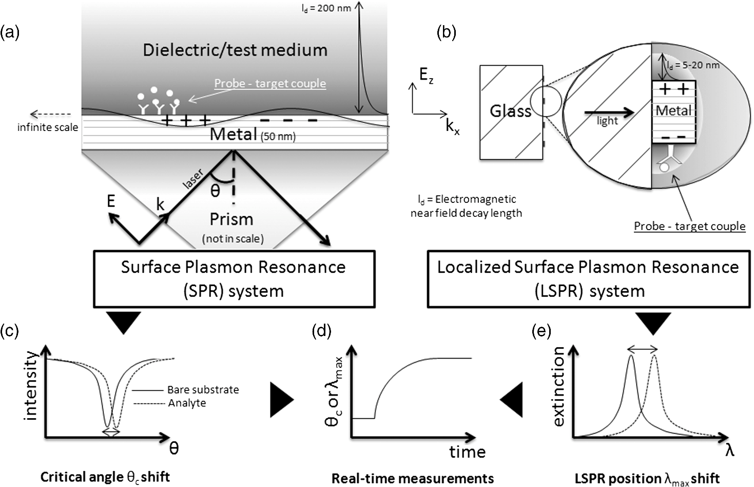 When the size of the metallic material is reduced to the nanometer scale, the SP cannot spread anymore because of the confinement imposed by the nanoparticle size [Fig. 7(b)]. These LSPs can be coupled directly to the incident light. Thus, unlike SPR sensors, there is no need of any additional component such as prism to excite and use the LSP. Each nanoparticle act as an individual sensor, however, the number of excited nanoparticles varies from several billion down to a single nanoparticle depending on the incident spot size. The lateral resolution provided by an LSPR sensor is thus much lower than for a SPR sensor.71 The order of magnitude of the LSPR sensor sensitivity is (two to four orders of magnitude lower than SPR sensors). However, the typical LSP decay length of 5 to 20 nm [Fig. 7(b)] makes the LSPR sensor less sensitive to interference from change in RI (due to a change in solution temperature) but more sensitive to any change very close to the surface.72,73 This drawback can be minimize since depends on the size and shape of the nanoparticles, which can be easily controlled by lithography techniques.67 In conclusion, LSPR sensors provide the same information than SPR sensors but with higher sensitivity for the detection of small RI change such as the binding of small molecules (molecular weight lower than ) or the binding of small quantity of molecule. A great advantage of LSPR is the possibility of miniaturization with the use of MNPs. For both SPR and LSPR sensors, any deposition of solvent or molecule on the metal induces an increase of the surrounding RI. In SPR or LSPR, the surrounding medium can be seen as a deposition of charges on the surface that damps the energy of the (L)SP. It then leads to a redshift of the (L)SPR position described in the case of solvent deposition by the following relationship:72 where is the bulk refractive index sensitivity (RIS) of the sensor (in nm/RIU) and is the change in the refractive index between two solvents. “Bulk” stands for a medium with a comparable size to the excitation wavelength in the three dimensions of space. Usually, the RIS is experimentally determined by measuring the LSPR wavelength shift induced by a change of the solvent RI [Fig. 8(a)]. The change of solvent (e.g., methanol: , water: , acetone: or heptanes: ) or concentration (few percent of sucrose in water or glycerol for example) is an easy way to tune the RI.74,75 The sensitivity is fully described by the figure of merit (FOM) defined as the ratio of over the full width at half maximum (FWHM) of the LSPR. Historically, has initially been defined in wavelength units per RIU, but in the literature, now-a-days is described using the resonance energy (i.e., eV/RIU). Even if the spectral range investigated in such experiment is narrow (550 to 900 nm), does not vary linearly with whatever the surrounding medium is (solvent or analyte monolayer), and thus is not constant on the whole spectral range. Equation (5) is simple since the surrounding medium seen by the nanoparticle has an infinite size. In the case of an analyte monolayer, depends strongly on the area probed by the electromagnetic near field created around the nanoparticle and characterized by its decay length . The expression of the LSPR shift assuming an exponential decay of the electromagnetic near field then becomes:76 where is now the change in refractive index between the analytes monolayer and the solvent and is the effective thickness of the layer made by adsorbed analytes (this thickness can be lower than the analyte size if the NP coverage is not complete).71,77,78 The thickness of the adsorbed layer and the surface coverage rate can be deduced from Eq. (6).Fig. 8(a) Schemes of the refractive index sensitivity (RIS) measurement principle showing the successive deposition of three different solvents on a MNP. The sensitivity m is also represented. (b) The successive steps for antigen (target) detection are depicted. A SAM is made on the bare metallic surface in order to fix the antibodies (probes) which then catch the antigens. The direction k and the associated electric field E are indicated and a representation of the electromagnetic near field is given in order to convince the reader of the necessity to control it and to choose very small SAM-probe couples.  The basis of biological sensing [Fig. 8(b)] is, first, the deposition of a SAM whose role is to capture the probe molecules closely to the MNPs surface since the molecule rarely binds naturally to the metal and to increase the sensor detection specificity. Commonly used SAMs for biosensing are composed of a thiol group, which can bind to the MNP (gold or silver), a carbon chain, and a functional group. Most often, this group is an amin () or carboxyl (COOH) that can easily bind to a biomolecule. For example, a common molecule used for such SAM is the 11-mercaptoundecanoic acid (MUA).79 In order to avoid any bonding of the probe or target molecule directly on the metallic surface, a blocking molecule such as octanthiol (OT) can be used.80 The main detection strategy in biological sensing is based on the couple antibody-antigen where either the antibody is attached to the SAM in order to catch selectively the corresponding antigen or the contrary. The chosen SAM-probe system has to be as small as possible since the detection is limited by the local electromagnetic field amplitude decay length. In such case, where is the effective refractive index of the three layers structure (SAM, probe, and target), and , the refractive index of the medium surrounding the structure. is obtained by integrating the distance-dependent local refractive index, , from zero to infinity:71 with , the RI at a distance from the surface such as: and with , the electromagnetic near field. The LSPR wavelengths shift measured after the deposition of the target is then written as: with and the LSPR wavelength measured, respectively, after the probe and the target deposition. One can thus deduce key information such as surface coverage and number of bond targets. Eventually, nonspecific binding studies [e.g., with Bovine Serum Albumin (BSA)] can be performed to verify that the response seen on the LSPR sensor is due to specific binding of the target to the probe molecule.81Before presenting the nanosensor applications, we would like to precise that all the nanoparticles geometries mentioned in the article are described in Fig. 9. More complex structures can also be found for example in the Refs. 82 and 83. Fig. 9Schemes of the nanoparticles or nanoholes geometries mentioned in this article (for each geometry, the left scheme is the side view and the right scheme is the top view). 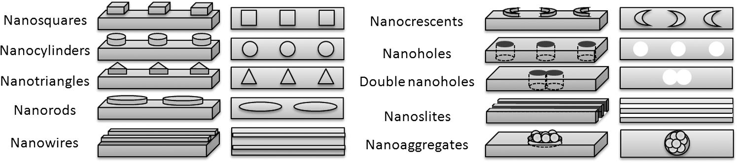 Using EBL substrates to act as biological sensors, Barbillon et al. employed the latter deposition strategy in order to detect antibiotin and streptavidin, which are known to have a strong affinity with biotin.83 A SAM of MUA was first deposited on 2D arrays of regularly spaced gold nanocylinders with 90 nm in diameter, 50 nm in height, and 250 nm between each nanoparticle. Biotin was then deposited on the SAM and used as probe to catch antibiotin and streptavidin separately. A limit of detection (LOD) of and even were, respectively, reached corresponding to few hundreds of streptavidin per nanocylinders. An application of such detection has also been demonstrated by Lin et al. using EBL to create equivalent arrays of nanocylinders (185 nm in diameter, 55 nm in height, and 400 nm between each nanoparticle) at the end of an optical fiber.84 A concentration of streptavidin as low as 6 pM has been detected. Piliarik et al. used arrays of nanorods (110 nm in length, 40 nm in width, 30 nm in height, and spaced by 150 nm) to detect the biotinylated oligonucleotide probed by streptavidin.85 An LOD of has been reached, which corresponds to less than one DNA molecule per nanoparticle. The RIS of the substrates described, here, are in the order of . EBL substrates have also been used as pH nanosensors by a direct exploitation of the RIS parameter. Jiang et al. designed arrays of gold randomly orientated nanocressents (260 nm in outer diameter, 80 nm in height, and 330 nm between each nanoparticles).86 The swelling property of hydrogel thin film deposited in the substrate was used to create a pH sensitive layer. The RIS was evaluated to and a detection sensitivity of 0.045 pH unit was reached. FIB is also used to create biological and chemical sensors since it is the main fabrication technique of periodic arrays of nanoholes in a metallic film (usually gold). Such samples have the particularity to provide an enhanced transmission of light through the holes known as extraordinary optical transmission (EOT) first reported in 1998 by Ebbesen et al.43 Even if several physical mechanisms are involved in EOT, it seems that SP play a major role (LSPR, Block wave SP polaritons in addition to Wood’s anomalies).87 The presence of such surface waves suggests that the transmission spectra are sensitive to any change of the local RI in the medium surrounding or inside the holes. Brolo et al. fabricated arrays of nanoholes in a gold film (200 nm in diameter, lattice periodicity of about 590 nm and 100 nm in gold thickness). They were used to monitor the binding of biological molecules (BSA) to the metallic surface.88 The RIS was evaluated to . Such substrate has been recently integrated with a micro-fluidic system to create an “on-chip” device measuring RI changes with a sensitivity and showed the ability to detect streptavidin using the couple cysteamin-biotin as probe layer.89 Another geometrical configuration has been exploited by Lee et al. who fabricated arrays of nanoslits (50 nm spaced, lattice periodicity of 600 nm, and 150 nm in gold thickness).90 A RIS of was measured by monitoring an antigen-antibody interaction. Large arrays of MNPs or nanoholes fabricated with NIL can be exploited as sensors. Barbillon et al. used arrays of gold nanocylinders produced by UV-NIL (165 nm in diameter, 30 nm in height, and spaced by 500 nm). This sample proved its ability as biological nanosensor through the detection of anti-biotin with a concentration of 10 µM and has shown a RIS of ( was estimated to be 31 nm).91 Lee et al. created arrays of gold nanoellipses (162 nm in length, 105 nm in width, 20 nm in height, and spaced by 340 nm) by T-NIL.92 They first showed an axis dependence of the RIS since a value of was measured for incident polarization along the long axis of the nanoellipses and along the short axis. They demonstrated the detection of a recombinant human prostate-specific antigen (PSA), which is a serum marker for the diagnosis of prostate cancer. MUA was first adsorbed on the nanoparticles before binding PSA antibodies. A LOD of was first reached. An enzyme-catalyzed precipitation method was then applied and showed an enhancement of the LOD, which became as low as . Due to an easy and low cost fabrication process, NSL is the most used nanolithography technique for sensing application. Most of the works presented below have been done with arrays of silver triangular nanoparticles with edge length of 100 nm and heights around 50 nm arranged in hexagonal array (nanosphere diameter: 400 nm). Such sample provides a RIS of . The couple biotin-streptavidin has been studied by Haes et al. MUA and OT were first adsorbed to the silver nanoparticles.84 Biotin then binds covalently to the carboxyl group of MUA just before exposition to streptavidin reaching a LOD below . Riboh et al. detected anti-biotin deposited on the same nanostructures-SAM-probe layer with a LOD of 93 and Hall et al. deposited gold nanoparticles on antibiotin to decrease the LOD to .94 Arrays of rhombic silver nanoparticles have been fabricated by Zhu et al. (140 nm in width and 47 nm in height) for biotin-streptavidin detection, they obtained a RIS of .95 A first multiplexing study in such sample has been done by Yonzon et al.85 A SAM was deposited on the nanoparticle surface just before binding two different probes proteins: mannose and galactose. When exposing the modified substrate to 19 µM concanavalin A (ConA, carbohydrate), a redshift was measured with mannose, wheareas no shift was observed on galactose. Such experiment could lead to the fabrication of carbohydrate sensing chips with multiple sugar arrays to investigate the binding of several proteins of interest simultaneously on a single chip. Amyloid -derived diffusible ligands (ADDL) and the anti-ADDL antibody are molecules possibly involved in the development of Alzheimer’s disease. These molecules have been detected with equivalent substrates by Haes et al. (edge size of 90 nm and nanoparticle height set to 30 nm). The couple MUA/OT was used as SAM layer with a coupling agent (the 1-ethyl-3-[3-dimethyl-aminopropyl]carbodiimide hydrochloride, EDC) to bind to ADDL and to form the probe layer. Anti-ADDL was then detected reaching a LOD of .96 Zhao et al. explored the possibility to combine the electronic resonance of molecules with the LSPR enabling the detection of low molecular weight targets.97 When resonant molecules are adsorbed on nanoparticles, the induced LSPR shift becomes strongly dependent on the spectral overlap between the electronic resonance of the molecule and the plasmon resonance of the nanoparticles. In this experiment, a drug sensor is created by using cytochrome P450 protein attached to MUA as probe layer (this probe is known to be inhibited by several drugs). An analyte with a molecular weight as low as (camphor, 200 µM concentration) has been detected. Das et al. did an equivalent work on identical substrates to detect 12 different drugs (e.g., bromocriptine, testosterone, or ketoconazole) with molecular weights ranging from 100 to .98 Recently, the Van Duyne’s group proposed the first label-free detection of protein conformation changes using array of silver nanotriangles (100 nm in length and 80 nm in height).99 A SAM with a terminal phosphonate group was immobilized to probe the calmodulin (a 19 kDa protein). The conformational change of the calmodulin protein was induced by cycles of exposition to a calcium ions based solution, which led the proteins to an “open” conformation inducing a LSPR redshift (about 1 nm). The chelation of the calcium ions lead to the reverse process and LSPR blueshift. Finally, NSL has been employed as chemical sensor of inert gas by detecting small changes in bulk refractive index as low as RIU when changing the gas from He(g) and Ar(g) and He(g) and .100 A summary of all these results are given in the Table 1. In each case, LSPR sensing was implemented with nanolithographied substrates. When evaluated by the authors, the RIS (chemical sensors) and LOD (biological sensors) are given. The LOD is defined as the sample concentration, which corresponds to the sensor response equal to three standard deviations of the sensor response to a blank sample.101 Table 1of LOD and RIS of LSPR sensors as a function of the MNPs parameters [lengths (L), widths (w), diameters (d), heights (h) and gaps (G)]. (m) are experimental values of the LOD. (–) is indicated when the information has not been given by the authors.
From Table 1, one can notice that an interesting number of analytes has been investigated with LSPR sensors. The most recent applications (with a medical interest) have been demonstrated using NSL substrates. LOD below are reached using nanolithographied substrates and a mean value of the RIS is located around even if better performance can be reached with substrates made by FIB. The coupling between metallic nanostructures is not really exploited even if such coupling could improve both the LOD and the RIS. However, the example of NSL substrates used for anti-ADDL sensing demonstrates sensitivity already relevant for clinical analysis. In conclusion, the choice of a lithography technique to make substrates for LSPR sensing depends mainly on the aim of the experiments (performance or a precise range of concentration to be reached). 4.2.SERS SensorSince the observation of a single molecule has been performed by SERS in 1997,102,103 a strong interest for the development of analytical tools based on SERS have been rekindled. The main advantage in the case of biosensors is that it is a label-free technique. SERS is based on an electromagnetic and a chemical effect. Here, we focus on the electromagnetic effect of SERS enabling an enhancement up to (the chemical effect104,105 providing an enhancement up to is not considered here).106,107 A. Wokaun explained in the 80’s that this effect comes from the electromagnetic interaction between a molecule and a MNP involving two distinct processes.8 The first one results in the interaction of the incident beam with the nanoparticle. It induces a local enhancement of the incident field (at a wavelength ) with a corresponding enhancement factor. The second process is explained by the interaction of the Raman signal with the MNP (at the wavelength which is shifted compared to ) and scattered by the molecule located at the vicinity of the nanoparticle surface. This second process induces an enhancement of the Raman signal (at ), called the re-radiation process with a corresponding enhancement factor . The final enhanced Raman intensity, , detected can thus be expressed as:108,109 where is the Raman intensity measured without the presence of metal and is the total electromagnetic enhancement factor (EF). Equation (10) shows that the total EF depends on the position of the LSPR wavelength compared to the excitation and the Raman wavelengths. As a consequence, nanolithographic techniques are particularly adapted for the optimization of SERS intensity, especially in the case of sensors. Many investigations have been carried out on nanolithographied substrates to show that: (i) the best SERS intensity in the case of arrays of gold nanocylinders (EBL, molecule deposited : ,2-bis(4-pyridyl)ethylene) 110,111 or silver nanotriangles (NSL, benzethiol based molecules)112 is obtained for a LSPR position located between the excitation ( in the visible range) and Raman wavelengths , (ii) this latter rule fails when choosing in the near-infrared (785 nm) in the case of arrays of gold nanocylinders with BPE as probe molecule, certainly due to non identical behaviors in the far field (LSPR) and in the near field (SERS) measurements113 (iii) in the case of elongated (e.g., ellipses, nanowires) gold nanoparticles, the lightning rod effect provided by such geometrical shapes favors the re-radiation process leading to a maximum of SERS intensity for a LSPR wavelength set close to 114 (iv) the polarization direction of strongly influences the SERS intensity in the case of non spherical nanoparticles114 (v) for larger nanoparticles (e.g., 200 nm for gold), higher orders of LSPR (non dipolar) appear.115,116 Not only they provide a contribution to the SERS intensity but a higher SERS intensity can be reached in the case of elongated nanoparticles.117,118 For cylindrical nanoparticles, no contribution of higher orders of LSPR in the SERS intensity has been observed118 (vi) the decay length plays a key role in the SERS process. has been probed for example by atomic layer deposition (ALD) of (one layer is 0.1 nm) as shown by the Van Duyne’s group on MFON substrates coated with silver (AgFON) made by NSL.119 A decrease by a factor of 10 of the SERS intensity of pyridine deposited on the alumina layers was observed after deposition of 2.8 nm of , thus leading to the same remark as for LSPR sensors i.e., the probe system (functionalization layer) has to be chosen as small as possible. (vii) The near field coupling between nanoparticles can significantly increase the SERS intensity up to two orders of magnitude as shown by Gunnarsson et al. (Rhodamin 6G and thiophenol deposited on arrays of silver nanocylinders made by EBL and with a nanoparticle gap decreasing from 500 nm to 70 nm) and confirmed by Liu et al. on the same substrate with BPE as probe molecule.120,121 A dependence of the SERS intensity inversely proportional to the 4th power of the nanoparticle gap was found.After the description of these key parameters studied on nanolithographied samples for the optimization of the SERS intensity, SERS applications for biological and chemical sensing will now be presented. DUV lithography substrates showed their ability as biological sensor and provided arrays of 3D silicon nanopillars with a square shape (around 100 nm in edge length) in which different thicknesses of silver (30 to 90 nm) are deposited. The distance (150 to 20 nm) and the sharpness of the squares have been changed by controlling the thickness of silver deposited and the exposure dosage, respectively, leading to the detection of 1 µM of Rhodamin 6G.122 Dinish et al. compared three different substrates in the purpose of glucose sensing. An AgFON like substrate made by DUV (called nanogap substrate with smallest gap close to 30 nm) was compared to AgFON substrate and to a commercial (Klarite) one. A mixed monolayer (dodecanthiol-mercaptohexanol) was used as SAM to deposit glucose on these substrates. A concentration of 5 mM was detected and estimated relevant for physiological conditions and a total EF of was estimated for the DUV substrates.123 In EBL, molecules such as test analytes have been used as proof of concept to determine the ability of the created substrates to act as biological sensor. BPE was deposited on arrays of gold nanocylinders114 and slightly elongated nanoparticles124 leading to EF of and , respectively. Yan et al. used p-mercaptoaniline (pMa) as test molecule on gold nanoparticle clusters arrays in cylinder shapes (diameter from 50 to 200 nm and gap fixed to 200 nm) providing an EF of .125 The same molecular probe was used to measure an enhancement of provided by deterministic aperiodic arrays of gold nanotriangles (edge length from 50 to 110 nm and gap from 25 to 100 nm).126 p-aminothiophenol has been deposited on a substrate made by EBL and an angle evaporation technique providing nanoparticles gap as low as 1 nm.127 These silver nanoparticles provided an enhancement of . Wells et al. employed another fabrication strategy using EBL to lithographically define nanoaggregates on which silver nanoparticles are deposited.128 Benzethiol has then been attached to silver nanoaggregates providing a EF. Equivalent substrates are based on drawing pattern on silicon layer with different shapes (circles or squares) and sizes (50 nm to 1 µm in length) and then deposit silver nanoparticles.129 In such experiments realized by Coluccio et al., a LOD as low as of Rhodamin 6G (R6G) has been detected. In the case of biosensors, EBL substrates such as arrays of gold nanocylinders (100 to 180 nm in diameter and gap fixed to 200 nm) have also been used to detect the BSA and Ribonuclease A proteins deposited with a concentration of 1 mM. A LOD of and was, respectively, estimated.130 BSA with MUA as probe layer has also been detected on arrays of coupled gold nanocylinders (100 nm in diameter and gap from 100 nm to fused dimers) with a concentration of 50 mM.131 The detection sensitivity showed a gain of a factor 6 from the noncoupled to coupled nanoparticles. Das et al. studied controlled gold nanograins (around 100 nm in diameter and gap from 10 to 30 nm) on which several proteins such as myoglobin were deposited.132 A LOD of was reached and could reach according to the author’s estimations. Moreover, a method enabling the classification of proteins by an analysis of their secondary structure was proposed.133 As shown in the LSPR sensors section, FIB is used to create arrays of nanoholes. As for LSPR sensors, the SERS performance is controlled by the size, the shape, the center to center gap, and the grating periodicity of the nanoholes. In the case of arrays of single gold nanoholes, Brolo et al. detected oxazine at a concentration of 10 µM.44 The gap was changed from 560 to 620 nm giving rise to the best performance for the lowest one. A comparison between arrays of gold nanocylinders and gold nanoholes has been made by Yu et al. for the detection of 4-mercaptopyridine.134 As a result, the best EF was reached for nanoholes ( for holes diameter of 350 nm and 500 nm gap). In order to enhance the SERS capabilities of nanoholes substrates, Lesuffleur et al. fabricated arrays of double nanoholes.46 When overlapping, two apexes are created and could be exploited for higher field enhancement. Optimized holes diameter as well as optimized periodicity of the double nanoholes arrays led to a gain of one order of magnitude of the SERS intensity of oxazine for each parameter comparing to the non overlapping case (corresponding to the sharpest apexes). Min et al. recently increased the performance of such substrate by exploiting an isolated gold double nanohole.135 This nanostructure showed a strong polarization dependence of the SERS intensity due to the symmetry of the double nanohole. As a result, a polarization set in the apex direction creates a confinement of the electromagnetic field. Thirteen hundred molecules were estimated to contribute to 60% of the SERS signal leading to a LOD of 20 molecules. Using NIL, Alvarez et al. created arrays of silver coated lines (150 nm in width and separated by 50 nm), nanosquares (125 nm in diameter) and nanoellipses of different aspect ratio (gap of 200 nm and height of 120 nm for all the nanostructure except the lines) in order to detect the 2-naphtalenthiol.136 Abu Hatab et al. fabricated arrays of silver squares, triangular, and elliptical nanocylinders (sizes ranging from 100 to 300 nm, 50 nm in height and nanocylinders gap of 100–200 nm).137 With such substrates, crystal violet and mitoxantrane were, respectively, detected at a LOD of and . A demonstration of application of SERS active substrate made by NIL has been done by Kostovski et al. with the design of arrays of silver nanocylinders at the tip of an optical fiber.138 First detection tests were done by the detection of 100 µM R6G and 10 mM ethanol. In the fabrication section, we explained that two kinds of substrates can be obtained by the NSL method. The first one provides arrays of MNPs of different geometrical parameters when the layer of nanospheres is removed after the metallic evaporation. The second one leads to MFON substrates for which the nanospheres layer has not been removed. Both methods provide easy making and cheap SERS active substrates. Those made of arrays of silver nanoparticles with triangular section have been exploited with test molecules to demonstrate their potential for biological sensing. Haynes et al. deposited monolayers of nonresonant (benzethiol molecules) and resonant () molecules for which EF of and were found, respectively (nanoparticle size of 100 nm and a height ranging from 25 to 40 nm).117 Other test molecules were adsorbed by Sweetenham et al. on such arrays with different geometrical parameters i.e., nanoparticle size of 230 nm and 40 nm in height.139 Rhodamin 6G was first deposited in order to measure the distribution field on the substrate and to show that most of the signal comes from the nanostructures themselves and not from their gaps. p-aminothiophenol (p-ATP) was then adsorbed to calculate the EF which reached . Lin et al. succeeded in the detection of the tetrodotoxin (scarce toxin with anesthesic properties) on equivalent arrays (nanoparticles size of 100 nm and 120 nm in height) and reached a LOD of .140 In the case of MFON substrates, BPE has been used as test molecule to evaluate the EF: nanospheres with a diameter of 542 nm and silver thickness of 200 nm have an average EF of . The random structure roughness that support LSPR contributed for to this enhancement and delocalized SP contributed for .141 Farcau et al. and Fang et al. probed the average and maximum EF obtained with such substrates. The first ones adsorbed a monoloayer of p-ATP on nanosphere with a diameter of 450 nm coated by a 100 nm thick gold film to find an average value of and a local one reaching .142 The second ones obtained an average value of and a local one reaching on a silver layer.143 Several important biological and chemical applications have been realized by the Van Duyne’s group with AgFON substrates. The research for glucose sensing was motivated by the development of a continuous monitoring device with a low degree of invasiveness. For this purpose, Shaffer et al. functionalized AgFON substrate (200 nm thick) with 1-decanethiol since the glucose does not bind naturally to silver.144 Such strategy succeeded to detect glucose in concentrations clinically relevant i.e., below 25 nM. Lyandres et al. then performed real-time and reversible glucose sensing in bovine plasma by an improvement of the SAM layer by using a mixture of decanethiol-mercaptohexanol.145 The last step was reached by Stuart et al. with in vivo application showing also real-time and reversible glucose measurements in a rat model (sensor implemented subcutaneously).146 Such strategy has been also exploited by Shah et al. for real-time and reversible detection of lactate (indicator of human performance levels, fatigue, and hydration) and physiological concentrations i.e., 6-240 ng.mL were reached. An Anthrax sensor was realized by Zhang et al. through the detection of bacillus spores.147 The silver surface of the AgFON substrate was modified with the deposition of alumina by ALD to reach a LOD of the spores of that is twice more sensitive than a direct spore deposition. AgFON substrates were also employed by Stuart et al. to detect in real-time chemical warfare agents such as half mustard gas catched by a decanethiol SAM.148 A summary of all these results are given in the Table 2. For each example given for SERS sensing with nanolithographied substrates and when evaluated by the authors, the sensors LOD and the EF are given. Table 2Values of LOD and Enhancement Factors (EF) of SERS sensors as a function of the MNPs parameters [lengths (L), widths (w), diameters (d), heights (h) and gaps (G)]. (*) are not LOD but concentrations relevant for the targeted application. (m) are experimental values of the LOD and (e) are estimated ones. (–) is indicated when the information has not been given by the authors.
Extremely low LOD can be reached using substrates made by nanolithography techniques (few molecules per MNP can be detected). Like for LSPR sensing, the choice in the nanolithography technique to make a SERS active substrate depends on the aim of the experiment (detection of a low concentration or a concentration range relevant for a specific application). Concerning the EFs presented, one has to pay attention to the way of calculation presented by the authors since the SERS intensity of a molecule is sometimes not compared to the “nonSERS” intensity from the same molecule. As expected, silver nanoparticles provides higher EFs than gold nanoparticles. MFON and aggregated substrates usually provide the best EFs. 4.3.MEF SensorsBasically, fluorescence consists in the absorption of one photon in the visible or UV range, which stimulates the emission of a second photon at lower energy. This phenomenon has long been and is still used for detection since it just exploits either the intrinsic fluorescence of the desired object or the fluorescence of a tag (fluorophore) that is labeled to the desired object. This physical process has been preferred for a long time to the Raman process since the latter one has a cross section; 12 to 14 orders of magnitude lower than the fluorescence one. The fluorescence phenomenon can also benefit from the field enhancement provided by MNPs and gives rise to MEF or surface enhanced fluorescence (SEF).149 The difference between the SERS and the SEF process is that both near and re-radiation fields participate to the final SERS intensity, whereas in SEF, the near field enhances only the absorption. As a consequence, there is a unique source of enhancement in SEF, which arises from the absorption step and increases the quantum yield (ratio between the emitted and absorbed photons). An enhancement in the range of 10 to 100 can be reached. However, the presence of the metal can induce the opposite effect named quenching and well known in fluorescence.150 For example, the emission of a fluorophore located within the first 5 nm from the metal surface is almost totally quenched. Systematic studies have been realized using EBL in order to find a compromise between the latter quenching effect and the enhancement. Corrigean et al. used arrays of silver nanotriangles and nanosquares (sizes ranging from 50 to 130 nm, center to center distance from 150 to 390 nm, and 80 nm in height).151 In order to avoid the quenching effect from a metallic surface, a spacer made of biotinylated BSA was deposited on the surface with an additional layer of avidin. Biotinylated fluorophores (fluorescein, Cy3 and Cy5) were then attached to the modified surface. The distance between silver and the fluorophore was estimated to be 9 nm using such spacer. As a result, the fluorescence enhancement was similar; whatever is the nanoparticle shape (square or triangles). For nanoparticle, center to center distance larger than 270 nm, the enhancement was similar to the one provided by a single silver nanoparticle. Thus, for lower gap down to 210 nm, the fluorescence enhancement increases, whereas it decreases below 210 nm due to the quenching effect. In this experiment, fluorescein and Cy3 gave the largest EF for nanoparticle edges (for squares and triangles) in the range of 85 to 95 nm (excitation wavelength of 488 and 514 nm), whereas a larger 110 nm nanoparticle was used for Cy5 to get a larger EF. The latter one was estimated to be in the order of 10 to 20. Guo et al. produced arrays of silver nanowires (length of several micrometers, width changed from 64 to 633 nm, center to center distance equal to twice the width, and 75 nm in height) and nanocolumns (square like shape with size identical to nanowires) by EBL.152 Cy3 and Cy5 fluorophores were deposited on the substrate using an equivalent spacing strategy as in the last example. An incident electric field polarization set perpendicular to the long nanowire axis provides a maximum enhancement for lateral spatial period of 0.65 times the excitation wavelength, whereas a polarization set along the nanowire axis provides no enhancement. In addition, the fluorescence enhancement was measured to be 4 times larger for nanocolumns than for nanowires. Evidence of the role of surface plasmon standing waves and Wood’s anomaly on the fluorescence enhancement process were given. Similar experiments have been realized by Szmacinzki et al. on arrays of silver nanocylinders, nanosquares, and nanotriangles (sizes ranging from 100 to 250 nm and 40, 65, and 90 nm gap lengths).153 Applications in biological sensing have been done for DNA detection by Liu et al. who used EBL to create gold nanocavities of 200 nm in diameter and 70 nm in gold thickness.154 This experiment gave rise to a real-time detection of 20 bases oligonucleotides in solution. The attomolar () concentration level of DNA has also been reached by De Angelis et al. by fabricating a 3D substrate made of a tip shaped nanostructure pointing out of the plane with a particular super-hydrophobicity property.42 Finally, Akashi et al. realized fluorescence images of labeled cells realized using T-NIL and UV-NIL substrates.155 As one can remark, the quantity of MEF experiments reported on 2D nanolithographied arrays of MNPs is limited and mainly using known and test molecule dyes. Even if systematic studies have been undertaken in order to improve the comprehension of the MEF phenomenon, more investigations are needed for this purpose and also for MEF sensors development. 5.ConclusionsThis review gave an overview of the investigations and applications realized on nanolithographied substrates for sensing purposes. A highlight of the key parameters governing the field enhancement efficiency has been given in order to understand why a precise control of the geometrical parameters of the MNPs is crucial. Two ways of detection, LSPR and SERS, are principally used for sensing with nanolithographied substrates and exploit the same localized surface wave phenomenon. For both, many proofs of concept have been realized with test molecules showing interesting performances such as LOD down to the attomolar level. Such sensors can thus compete with ELISA or quartz crystal microbalance systems. However, even if some experiments succeeded in creating recent applications using nanolithographied substrates, such as glucose or anthrax sensors, there are still very few of them presenting the detection of biologic molecules (e.g., biomarkers) of traces of chemical or of explosives for example or even some ways to monitor nanoscale biological or chemical phenomena. The use of nanolithographied substrates can therefore provide some promising applications, but there is still a long way to do to develop them. AcknowledgmentsThe authors want to acknowledge the Nanoantenna’s project (FP7-HEALTH-F5-2009-241818-NANOANTENNA) for financial support. ReferencesH. K. Kleinmanet al.,
“Biological-activities of laminin,”
J. Cell. Biochem., 27
(4), 317
–325
(1985). http://dx.doi.org/10.1002/(ISSN)1097-4644 JCEBD5 0730-2312 Google Scholar
J. RickertA. BrechtW. Gopel,
“Quartz crystal microbalances for quantitative biosensing and characterizing protein multilayers,”
Biosens. Bioelectron., 12
(7), 567
–575
(1997). http://dx.doi.org/10.1016/S0956-5663(96)00077-2 BBIOE4 0956-5663 Google Scholar
Z. Caoet al.,
“An EQCM study on the interaction of heparin with the charge-transfer complex generated during o-tolidine electrooxidation: a biosensing mode with a dynamically renewed surface,”
Biosens. Bioelectron., 23
(3), 348
–354
(2007). http://dx.doi.org/10.1016/j.bios.2007.04.016 BBIOE4 0956-5663 Google Scholar
N. GuillotM. L. de la Chapelle,
“Nanoantenna,”
Encyclopedia of Electrical and Electronics Engineering, Wiley, New York
(2012). Google Scholar
G. Mie,
“Beiträge zur optik trüber medien, speziell kolloidaler metallösungen,”
Ann. Physik., 330 377
–445
(1908). http://dx.doi.org/10.1002/(ISSN)1521-3889 ANPYA2 0003-3804 Google Scholar
C. F. BohrenD. R. Huffman, Absorption and Scattering of Light by Small Particles, Wiley, New York
(1983). Google Scholar
P. B. JohnsonR. W. Christy,
“Optical constants of noble metals,”
Phys. Rev. B, 6
(12), 4370
–4379
(1972). http://dx.doi.org/10.1103/PhysRevB.6.4370 PRBMDO 0163-1829 Google Scholar
A. Wokaun,
“Surface-enhanced electromagnetic processes,”
Solid State Phys., 38 223
–294
(1984). http://dx.doi.org/10.1016/S0081-1947(08)60314-8 SSPHAE 0081-1947 Google Scholar
M. MeierA. Wokaun,
“Enhanced fields on large metal particles: dynamic depolarization,”
Opt. Lett., 8
(11), 581
–583
(1983). http://dx.doi.org/10.1364/OL.8.000581 OPLEDP 0146-9592 Google Scholar
A. WokaunJ. P. GordonP. F. Liao,
“Radiation damping in surface-Enhanced Raman scattering,”
Phys. Rev. Lett., 48
(14), 957
–960
(1982). http://dx.doi.org/10.1103/PhysRevLett.48.957 PRLTAO 0031-9007 Google Scholar
B. Lamprechtet al.,
“Metal nanoparticle gratings: influence of dipolar particle interaction on the plasmon resonance,”
Phys. Rev. Lett., 84
(20), 4721
–4724
(2000). http://dx.doi.org/10.1103/PhysRevLett.84.4721 PRLTAO 0031-9007 Google Scholar
J. KottmannO. Martin,
“Retardation-induced plasmon resonances in coupled nanoparticles,”
Opt. Lett., 26
(14), 1096
–1098
(2001). http://dx.doi.org/10.1364/OL.26.001096 OPLEDP 0146-9592 Google Scholar
Z. Liuet al.,
“Plasmonic nanoantenna arrays for the visible,”
Metamaterials, 2
(1), 45
–51
(2008). http://dx.doi.org/10.1016/j.metmat.2008.03.001 1873-1988 Google Scholar
W. Rechbergeret al.,
“Optical properties of two interacting gold nanoparticles,”
Opt. Comm., 220
(1–3), 137
–141
(2003). http://dx.doi.org/10.1016/S0030-4018(03)01357-9 OPCOB8 0030-4018 Google Scholar
C. TaborD. Van HauteM. A. El-Sayed,
“Effect of orientation on plasmonic coupling between gold nanorods,”
ACS Nano, 3
(11), 3670
–3678
(2009). http://dx.doi.org/10.1021/nn900779f 1936-0851 Google Scholar
J. Alegretet al.,
“Plasmonic properties of silver trimers with trigonal symmetry fabricated by electron-beam lithography,”
J. Phys. Chem. C, 112
(37), 14313
–14317
(2008). http://dx.doi.org/10.1021/jp804505k 1932-7447 Google Scholar
S. MaierM. L. BrongersmaH. A. Atwater,
“Observation of near-field coupling in metal nanoparticle chains using far-field polarization spectroscopy,”
Phys. Rev. B, 65
(19), 193408
(2002). http://dx.doi.org/10.1103/PhysRevB.65.193408 PRBMDO 1098-0121 Google Scholar
P. K. JainW. HuangM. A. El-Sayed,
“On the universal scaling behavior of the distance decay of plasmon coupling in metal nanoparticle Pairs: a plasmon ruler equation,”
Nano Lett., 7
(7), 2080
–2088
(2007). http://dx.doi.org/10.1021/nl071008a NALEFD 1530-6984 Google Scholar
P. K. JainM. A. El-Sayed,
“Surface plasmon coupling and its universal size scaling in metal nanostructures of complex geometry: elongated particle pairs and nanosphere trimers,”
J. Phys. Chem. C, 112
(13), 4954
–4960
(2008). http://dx.doi.org/10.1021/jp7120356 1932-7447 Google Scholar
P. K. JainM. A. El-Sayed,
“Plasmonic coupling in noble metal nanostructures,”
Chem. Phys. Lett., 487
(4–6), 153
–164
(2010). http://dx.doi.org/10.1016/j.cplett.2010.01.062 CHPLBC 0009-2614 Google Scholar
R. Weissleder,
“A clearer vision for in vivo imaging,”
Nat. Biotech., 19 316
–317
(2001). http://dx.doi.org/10.1038/86684 NABIF9 1087-0156 Google Scholar
C. Zheng,
“Nanofabrication by photons,”
Nanofabrication Principles, Capabilities and Limites, 7
–73 Springer, US
(2009). Google Scholar
J. L. Burn,
“Optical lithography—present and future challenges,”
C. R. Physique, 7
(8), 858
–874
(2006). http://dx.doi.org/10.1016/j.crhy.2006.10.005 CRPOBN 1631-0705 Google Scholar
R. Z. Tanet al.,
“3D arrays of SERS substrate for ultrasensitive molecular detection,”
Sens. Actuat. A Phys., 139
(1–2), 36
–41
(2007). http://dx.doi.org/10.1016/j.sna.2006.11.010 SAAPEB 0924-4247 Google Scholar
U. S. Dinishet al.,
“Development of highly reproducible nanogap SERS substrates: comparative performance analysis and its application for glucose sensing,”
Biosens. Bioelec., 26
(5), 1987
–1992
(2011). http://dx.doi.org/10.1016/j.bios.2010.08.069 BBIOE4 0956-5663 Google Scholar
M. J. WordI. AdesidaP. R. Berger,
“Nanometer-period gratings in hydrogen silsesquioxane fabricated by electron beam lithography,”
J. Vac. Sci. Technol. B, 21
(6), L12
(2003). http://dx.doi.org/10.1116/1.1629711 JVTBD9 0734-211X Google Scholar
K. YamazakiH. Namatsu,
“5-nm-order electron-beam lithography for nanodevice fabrication,”
Jpn. J. Appl. Phys., 43 3767
–3771
(2004). http://dx.doi.org/10.1143/JJAP.43.3767 JJAPA5 0021-4922 Google Scholar
C. Zheng,
“Nanofabrication by charged beams,”
Nanofabrication Principles, Capabilities and Limites, 77
–124 Springer, US
(2009). Google Scholar
J. Grandet al.,
“Role of localized surface plasmons in surface-enhanced Raman scattering of shape-controlled metallic particles in regular arrays,”
Phys. Rev. B, 72
(3), 33407
(2005). http://dx.doi.org/10.1103/PhysRevB.72.033407 PRBMDO 0163-1829 Google Scholar
E. C. Le Ruet al.,
“Surface enhanced Raman spectroscopy on nanolithography-prepared substrates,”
Curr. Appl. Phys., 8
(3–4), 467
–470
(2008). http://dx.doi.org/10.1016/j.cap.2007.10.073 Google Scholar
A. Clearyet al.,
“Fabrication of double split metallic nanorings for Raman sensing,”
Microelectron. Eng., 86
(4–6), 1146
–1149
(2009). http://dx.doi.org/10.1016/j.mee.2009.02.008 MIENEF 0167-9317 Google Scholar
G. Laurentet al.,
“Probing surface plasmon fields by far-field Raman imaging,”
J. Microsc., 229
(2), 189
–196
(2008). http://dx.doi.org/10.1111/j.1365-2818.2008.01885.x JMICAR 0022-2720 Google Scholar
S. S. Aćimovićet al.,
“Plasmon near-field coupling in metal dimers as a step toward single-molecule sensing,”
ACS Nano, 3
(5), 1231
–1237
(2009). http://dx.doi.org/10.1021/nn900102j 1936-0851 Google Scholar
S. Tripathyet al.,
“Acousto-plasmonic and surface-enhanced Raman scattering properties of coupled gold nanospheres/nanodisk trimers,”
Nano Lett., 11
(2), 431
–437
(2011). http://dx.doi.org/10.1021/nl103089e NALEFD 1530-6984 Google Scholar
L. Gunnarssonet al.,
“Interparticle coupling effects in nanofabricated substrates for surface-enhanced Raman scattering,”
Appl. Phys. Lett., 78
(6), 802
–804
(2001). http://dx.doi.org/10.1063/1.1344225 APPLAB 0003-6951 Google Scholar
H. Duanet al.,
“Direct and reliable patterning of plasmonic nanostructures with sub-10-nm gaps,”
ACS Nano, 5
(9), 7593
–7600
(2011). http://dx.doi.org/10.1021/nn2025868 1936-0851 Google Scholar
M. G. BanaeeK. B. Crozier,
“Mixed dimer double-resonance substrates for surface-enhanced Raman spectroscopy,”
ACS Nano, 5
(1), 307
–314
(2011). http://dx.doi.org/10.1021/nn102726j 1936-0851 Google Scholar
A. Gopinathet al.,
“Deterministic aperiodic arrays of metal nanoparticles for surface-enhanced Raman scattering (SERS),”
Opt. Express, 17
(5), 3741
–3753
(2009). http://dx.doi.org/10.1364/OE.17.003741 OPEXFF 1094-4087 Google Scholar
S. M. Wellset al.,
“Controllable nanofabrication of aggregate-like nanoparticle substrates and evaluation for surface-enhanced Raman spectroscopy,”
ACS Nano, 3
(12), 3845
–3853
(2009). http://dx.doi.org/10.1021/nn9010939 1936-0851 Google Scholar
G. Daset al.,
“Nano-patterned SERS substrate: application for protein analysis vs. temperature,”
Biosens. Bioelec., 24
(6), 1693
–1699
(2009). http://dx.doi.org/10.1016/j.bios.2008.08.050 BBIOE4 0956-5663 Google Scholar
F. De Angeliset al.,
“Breaking the diffusion limit with super-hydrophobic delivery of molecules to plasmonic nanofocusing SERS structures,”
Nat. Photon., 5 682
–687
(2011). http://dx.doi.org/10.1038/nphoton.2011.222 1749-4885 Google Scholar
T. W. Ebbesenet al.,
“Extraordinary optical transmission through sub-wavelength hole arrays,”
Nature, 391 667
–669
(1998). http://dx.doi.org/10.1038/35570 NATUAS 0028-0836 Google Scholar
J. DintingerT. W. Ebbesen,
“Molecule–surface plasmon interactions in hole arrays: enhanced absorption, refractive index changes, and all-optical switching,”
Adv. mat., 18
(10), 1267
–1270
(2006). http://dx.doi.org/10.1002/(ISSN)1521-4095 ADVMEW 0935-9648 Google Scholar
A. Lesuffleuret al.,
“Apex-enhanced Raman spectroscopy using double-hole arrays in a gold film,”
J. Phys. Chem. C, 111
(6), 2347
–2350
(2007). http://dx.doi.org/10.1021/jp067677e 1932-7447 Google Scholar
K.-L. Leeet al.,
“Sensitive biosensor array using surface plasmon resonance on metallic nanoslits,”
J. Biomed. Opt., 12
(4), 044023
(2007). http://dx.doi.org/10.1117/1.2772296 JBOPFO 1083-3668 Google Scholar
F. Lopez-Tejeiraet al.,
“Efficient unidirectional nanoslit couplers for surface plasmons,”
Nat. Phys., 3 324
–328
(2007). http://dx.doi.org/10.1038/nphys584 NPAHAX 1745-2473 Google Scholar
V. S. Volkovet al.,
“Wavelength selective nanophotonic components utilizing channel plasmon polaritons,”
Nano Lett., 7
(4), 880
–884
(2007). http://dx.doi.org/10.1021/nl070209b NALEFD 1530-6984 Google Scholar
S. Y. ChouP. R. KraussP. J. Renstrom,
“Imprint of sub-25 nm vias and trenches in polymers,”
Appl. Phys. Lett., 67
(21), 3114
–3116
(1995). http://dx.doi.org/10.1063/1.114851 APPLAB 0003-6951 Google Scholar
E. A. Costneret al.,
“Nanoimprint lithography materials development for semiconductor device fabrication,”
Annu. Rev. Mater. Res., 39 155
–180
(2009). http://dx.doi.org/10.1146/annurev-matsci-082908-145336 ARMRCU 1531-7331 Google Scholar
J. Haismaet al.,
“Mold-assisted nanolithography: a process for reliable pattern replication,”
J. Vac. Sci. Technol. B, 14
(6), 4124
(1996). http://dx.doi.org/10.1116/1.588604 JVTBD9 0734-211X Google Scholar
R. Alvarez-Pueblaet al.,
“Nanoimprinted SERS-active substrates with tunable surface plasmon resonances,”
J. Phys. Chem. C, 111
(18), 6720
–6723
(2007). http://dx.doi.org/10.1021/jp070906s 1932-7447 Google Scholar
S.-W. Leeet al.,
“Highly sensitive biosensing using arrays of plasmonic Au nanodisks realized by nanoimprint lithography,”
ACS Nano, 5
(2), 897
–904
(2011). http://dx.doi.org/10.1021/nn102041m 1936-0851 Google Scholar
S. Y. Chouet al.,
“Sub-10 nm imprint lithography and applications,”
J. Vac. Sci. Technol. B, 15
(6), 2897
(1997). http://dx.doi.org/10.1116/1.589752 JVTBD9 0734-211X Google Scholar
U. C. FischerH. P. Zingsheim,
“Submicroscopic pattern replication with visible light,”
J. Vac. Sci. Technol., 19
(4), 881
(1981). http://dx.doi.org/10.1116/1.571227 JVSTAL 0022-5355 Google Scholar
H. W. DeckmanJ. H. Dunsmuir,
“Natural lithography,”
Appl. Phys. Lett., 41
(4), 377
(1982). http://dx.doi.org/10.1063/1.93501 APPLAB 0003-6951 Google Scholar
J. C. HulteenR. P. Van Duyne,
“Nanosphere lithography: a materials general fabrication process for periodic particle array surfaces,”
J. Vac. Sci. Technol. A, 13
(3), 1553
–1558
(1995). http://dx.doi.org/10.1116/1.579726 JVTAD6 0734-2101 Google Scholar
J. C. Hulteenet al.,
“Nanosphere lithography: size-tunable silver nanoparticle and surface cluster arrays,”
J. Phys. Chem. B, 103
(19), 3854
–3863
(1999). http://dx.doi.org/10.1021/jp9904771 JPCBFK 1520-6106 Google Scholar
C. L. HaynesR. P. Van Duyne,
“Nanosphere lithography: a versatile nanofabrication tool for studies of size-dependent nanoparticle optics,”
J. Phys. Chem. B, 105
(24), 5599
–5611
(2001). http://dx.doi.org/10.1021/jp010657m JPCBFK 1520-6106 Google Scholar
J. N. Ankeret al.,
“Biosensing with plasmonic nanosensors,”
Nat. Mater., 7 442
–453
(2008). http://dx.doi.org/10.1038/nmat2162 NMAACR 1476-1122 Google Scholar
W. Yanget al.,
“A surface-enhanced hyper-Raman and surface-enhanced Raman scattering study of trans-1,2-bis (4-pyridyl) ethylene adsorbed onto silver film over nanosphere electrodes. Vibrational assignments: experiment and theory,”
J. Chem. Phys., 104
(11), 4313
–4323
(1996). http://dx.doi.org/10.1063/1.471241 JCPSA6 0021-9606 Google Scholar
D. A. Stuartet al.,
“In vivo glucose measurement by surface-enhanced Raman spectroscopy,”
Anal. Chem., 78
(20), 7211
–7215
(2006). http://dx.doi.org/10.1021/ac061238u ANCHAM 0003-2700 Google Scholar
J. J. Baumberget al.,
“Angle-resolved surface-enhanced Raman scattering on metallic nanostructured plasmonic crystals,”
Nano Lett., 5
(11), 2262
–2267
(2005). http://dx.doi.org/10.1021/nl051618f NALEFD 1530-6984 Google Scholar
T. A. Kelfet al.,
“Localized and delocalized plasmons in metallic nanovoids,”
Phys. Rev. B, 74
(24), 245415
(2006). http://dx.doi.org/10.1103/PhysRevB.74.245415 PRBMDO 0163-1829 Google Scholar
A. J. Haeset al.,
“Nanoscale optical biosensor: short range distance dependence of the localized surface plasmon resonance of noble metal nanoparticles,”
J. Phys. Chem. B, 108
(22), 6961
–6968
(2004). http://dx.doi.org/10.1021/jp036261n JPCBFK 1520-6106 Google Scholar
A. J. Haeset al.,
“A nanoscale optical biosensor: the long range distance dependence of the localized surface plasmon resonance of noble metal nanoparticles,”
J. Phys. Chem. B, 108
(1), 109
–116
(2004). http://dx.doi.org/10.1021/jp0361327 JPCBFK 1520-6106 Google Scholar
C. R. Yonzonet al.,
“Towards advanced chemical and biological nanosensors—an overview,”
Talanta, 67
(3), 438
–448
(2005). http://dx.doi.org/10.1016/j.talanta.2005.06.039 TLNTA2 0039-9140 Google Scholar
J. Homola,
“Surface plasmon resonance sensors for detection of chemical and biological species,”
Chem. Rev., 108
(2), 462
–493
(2008). http://dx.doi.org/10.1021/cr068107d CHREAY 0009-2665 Google Scholar
I. Abdulhalim,
“Enhanced spectroscopies and surface plasmon thin film sensors,”
Plasmonics, Functionalization and Biosensing, Pan Stanford Publishing, Singapore
(2011). Google Scholar
L. S. Junget al.,
“Quantitative interpretation of the response of surface plasmon resonance sensors to adsorbed films,”
Langmuir, 14
(19), 5636
–5648
(1998). http://dx.doi.org/10.1021/la971228b LANGD5 0743-7463 Google Scholar
A. HaesR. P. Van Duyne,
“A unified view of propagating and localized surface plasmon resonance biosensors,”
Anal. Bioanal. Chem., 379
(7–8), 920
–930
(2004). http://dx.doi.org/10.1007/s00216-004-2708-9 ABCNBP 1618-2642 Google Scholar
A. D. McFarlandR. P. Van Duyne,
“Single silver nanoparticles as real-time optical sensors with zeptomole sensitivity,”
Nano Lett., 3
(8), 1057
–1062
(2003). http://dx.doi.org/10.1021/nl034372s NALEFD 1530-6984 Google Scholar
D. E. Charleset al.,
“Versatile solution phase triangular silver nanoplates for highly sensitive plasmon resonance sensing,”
ACS Nano, 4
(1), 55
–64
(2010). http://dx.doi.org/10.1021/nn9016235 1936-0851 Google Scholar
G. Barbillonet al.,
“Sensitive detection of biological species through localized surface-plasmon resonance on gold nanodisks,”
Thin Solid Films, 517
(9), 2997
–3000
(2009). http://dx.doi.org/10.1016/j.tsf.2008.11.072 THSFAP 0040-6090 Google Scholar
Y. Linet al.,
“E-beam patterned gold nanodot arrays on optical fiber tips for localized surface plasmon resonance biochemical sensing,”
Sensors, 10
(10), 9397
–9406
(2010). http://dx.doi.org/10.3390/s101009397 SNSRES 0746-9462 Google Scholar
S.-W. Leeet al.,
“Highly sensitive biosensing using arrays of plasmonic Au nanodisks realized by nanoimprint lithography,”
ACS Nano, 5
(2), 897
–904
(2011). http://dx.doi.org/10.1021/nn102041m 1936-0851 Google Scholar
K. A. WilletsR. P. Van Duyne,
“Localized surface plasmon resonance spectroscopy and sensing,”
Annu. Rev. Phys. Chem., 58 267
–297
(2007). http://dx.doi.org/10.1146/annurev.physchem.58.032806.104607 ARPLAP 0066-426X Google Scholar
E. PetryayevaU. J. Krull,
“Localized surface plasmon resonance: Nanostructures, bioassays and biosensing—a review,”
Analytica Chimica Acta, 706
(1), 8
–24
(2011). http://dx.doi.org/10.1016/j.aca.2011.08.020 ACACAM 0003-2670 Google Scholar
L. B. Sagleet al.,
“Advances in localized surface plasmon resonance biosensing,”
Nanomedicine, 6
(8), 1447
–1462
(2011). http://dx.doi.org/10.2217/nnm.11.117 1743-5889 Google Scholar
G. Barbillonet al.,
“Sensitive detection of biological species through localized surface-plasmon resonance on gold nanodisks,”
Thin Solid Films, 517
(9), 2997
–3000
(2009). http://dx.doi.org/10.1016/j.tsf.2008.11.072 THSFAP 0040-6090 Google Scholar
A. J. HaesR. P. Van Duyne,
“A nanoscale optical biosensor: sensitivity and selectivity of an approach based on the localized surface plasmon resonance spectroscopy of triangular silver nanoparticles,”
J. Am. Chem. Soc., 124
(35), 10596
–10604
(2002). http://dx.doi.org/10.1021/ja020393x JACSAT 0002-7863 Google Scholar
C. R. Yonzonet al.,
“A comparative analysis of localized and propagating surface plasmon resonance sensors: the binding of concanavalin A to a monosaccharide functionalized self-assembled monolayer,”
J. Am. Chem. Soc., 126
(39), 12669
–12676
(2004). http://dx.doi.org/10.1021/ja047118q JACSAT 0002-7863 Google Scholar
S. Kaleleet al.,
“ Plasmon-assisted photonics at the nanoscale,”
J. Nanophoton., 1 12501
(2007). http://dx.doi.org/10.1117/1.2748429 JNOACQ 1934-2608 Google Scholar
G. Pavan Kumar,
“Plasmonic nano-architectures for surface enhanced Raman scattering: a review,”
J. Nanophoton., 6 64503
(2012). http://dx.doi.org/10.1117/1.JNP.6.064503 JNOACQ 1934-2608 Google Scholar
Y. Linet al.,
“E-Beam patterned gold nanodot arrays on optical fiber tips for localized surface plasmon resonance biochemical sensing,”
Sensors, 10
(10), 9397
–9406
(2010). http://dx.doi.org/10.3390/s101009397 SNSRES 0746-9462 Google Scholar
M. Piliariket al.,
“High-resolution biosensor based on localized surface plasmons,”
Opt. Express, 20
(1), 672
–680
(2012). http://dx.doi.org/10.1364/OE.20.000672 OPEXFF 1094-4087 Google Scholar
H. JiangJ. MarkowskiJ. Sabarinathan,
“Near-infrared optical response of thin film pHsensitive hydrogel coated on a gold nanocrescent array,”
Opt. Express, 17
(24), 21802
–21807
(2009). http://dx.doi.org/10.1364/OE.17.021802 OPEXFF 1094-4087 Google Scholar
S.-H. ChangS. GrayG. C. Schatz,
“Surface plasmon generation and light transmission by isolated nanoholes and arrays of nanoholes in thin metal films,”
Opt. Express, 13
(8), 3150
–3165
(2005). http://dx.doi.org/10.1364/OPEX.13.003150 OPEXFF 1094-4087 Google Scholar
A. G. Broloet al.,
“Surface plasmon sensor based on the enhanced light transmission through arrays of nanoholes in gold films,”
Langmuir, 20
(12), 4813
–4815
(2004). http://dx.doi.org/10.1021/la0493621 LANGD5 0743-7463 Google Scholar
A. De Leebeecket al.,
“On-chip surface-based detection with nanohole arrays,”
Anal. Chem., 79
(11), 4094
–4100
(2007). http://dx.doi.org/10.1021/ac070001a ANCHAM 0003-2700 Google Scholar
K.-L. Leeet al.,
“Sensitive biosensor array using surface plasmon resonance on metallic nanoslits,”
J. Biomed. Opt., 12 044023
(2007). http://dx.doi.org/10.1117/1.2772296 JBOPFO 1083-3668 Google Scholar
G. Barbillonet al.,
“Gold nanoparticles by soft UV nanoimprint lithography coupled to a lift-off process for plasmonic sensing of antibodies,”
Microelectron. Eng., 87
(5–8), 1001
–1004
(2010). http://dx.doi.org/10.1016/j.mee.2009.11.114 MIENEF 0167-9317 Google Scholar
S.-W. Leeet al.,
“Highly sensitive biosensing using arrays of plasmonic Au nanodisks realized by nanoimprint lithography,”
ACS Nano, 5
(2), 897
–904
(2011). http://dx.doi.org/10.1021/nn102041m 1936-0851 Google Scholar
J. C. Ribohet al.,
“A nanoscale optical biosensor: real-time immunoassay in physiological buffer enabled by improved nanoparticle adhesion,”
J. Phys. Chem. B, 107
(8), 1772
–1780
(2003). http://dx.doi.org/10.1021/jp022130v JPCBFK 1520-6106 Google Scholar
W. HallS. N. NgatiaR. P. Van Duyne,
“LSPR biosensor signal enhancement using nanoparticle—antibody conjugates,”
J. Phys. Chem. C, 115
(5), 1410
–1414
(2011). http://dx.doi.org/10.1021/jp106912p 1932-7447 Google Scholar
S. ZhuC. DuY. Fu,
“Fabrication and characterization of rhombic silver nanoparticles for biosensing,”
Opt. Mater., 31
(6), 769
–774
(2009). http://dx.doi.org/10.1016/j.optmat.2008.07.014 OMATET 0925-3467 Google Scholar
A. J. Haeset al.,
“A localized surface plasmon resonance biosensor: first steps toward an assay for Alzheimer’s disease,”
Nano Lett., 4
(6), 1029
–1034
(2004). http://dx.doi.org/10.1021/nl049670j NALEFD 1530-6984 Google Scholar
J. Zhaoet al.,
“Resonance surface plasmon spectroscopy: low molecular weight substrate binding to cytochrome P450,”
J. Am. Chem. Soc., 128
(34), 11004
–11005
(2006). http://dx.doi.org/10.1021/ja0636082 JACSAT 0002-7863 Google Scholar
A. Daset al.,
“Screening of type I and II drug binding to human cytochrome P450-3A4 in nanodiscs by localized surface plasmon resonance spectroscopy,”
Anal. Chem., 81
(10), 3754
–3759
(2009). http://dx.doi.org/10.1021/ac802612z ANCHAM 0003-2700 Google Scholar
W. P. Hallet al.,
“A conformation- and ion-sensitive plasmonic biosensor,”
Nano Lett., 11
(3), 1098
–1105
(2011). http://dx.doi.org/10.1021/nl103994w NALEFD 1530-6984 Google Scholar
J. M. Bingham,
“Gas sensing with high-resolution localized surface plasmon resonance spectroscopy,”
J. Phys. Chem. B, 132
(49), 17358
–17359
(2010). http://dx.doi.org/10.1021/ja1074272 JPCBFK 1520-6106 Google Scholar
J. Homola, Surface Plasmon Resonance Based Sensors, Springer-Verlag, Berlin-Heidelberg-New York
(2006). Google Scholar
K. Kneippet al.,
“Single molecule detection using surface-enhanced Raman scattering (SERS),”
Phys. Rev. Lett., 78
(9), 1667
–1670
(1997). http://dx.doi.org/10.1103/PhysRevLett.78.1667 PRLTAO 0031-9007 Google Scholar
S. NieS. R. Emory,
“Probing single molecules and single nanoparticles by surface-enhanced Raman scattering,”
Science, 275
(5303), 1102
–1106
(1997). http://dx.doi.org/10.1126/science.275.5303.1102 SCIEAS 0036-8075 Google Scholar
A. OttoJ. TimperI. Pockrand,
“Enhanced inelastic light scattering from metal electrodes caused by adatoms,”
Phys. Rev. Lett., 45
(1), 46
–49
(1980). http://dx.doi.org/10.1103/PhysRevLett.45.46 PRLTAO 0031-9007 Google Scholar
A. CampionP. Kambhampati,
“Surface-enhanced Raman scattering,”
Chem. Soc. Rev., 27 241
–250
(1998). http://dx.doi.org/10.1039/a827241z CSRVBR 0306-0012 Google Scholar
H. Xuet al.,
“Spectroscopy of single hemoglobin molecules by surface enhanced Raman scattering,”
Phys. Rev. Lett., 83
(21), 4357
–4360
(1999). http://dx.doi.org/10.1103/PhysRevLett.83.4357 PRLTAO 0031-9007 Google Scholar
E. C. Le Ruet al.,
“Surface enhanced Raman scattering enhancement factors: a comprehensive study,”
J. Phys. Chem. C, 111
(37), 13794
–13803
(2007). http://dx.doi.org/10.1021/jp0687908 1932-7447 Google Scholar
A. Wokaun,
“Surface-enhanced electromagnetic processes,”
Solid State Phys., 38 223
–294
(1984). http://dx.doi.org/10.1016/S0081-1947(08)60314-8 SSPHAE 0081-1947 Google Scholar
E. C. Le RuP. G. Etchegoin,
“SERS enhancement factors and related topics. Principles of surface-enhanced Raman spectroscopy,”
Principles of Surface Enhanced Raman Scattering, 185
–264 Elsevier, Amsterdam
(2009). Google Scholar
N. Félidjet al.,
“Controlling the optical response of regular arrays of gold particles for surface-enhanced Raman scattering,”
Phys. Rev. B, 65
(7), 075419
(2002). http://dx.doi.org/10.1103/PhysRevB.65.075419 PRBMDO 1098-0121 Google Scholar
J. Grandet al.,
“Optimization of SERS-active substrates for near-field Raman spectroscopy,”
Synth. Met., 139
(3), 621
–624
(2003). http://dx.doi.org/10.1016/S0379-6779(03)00276-5 SYMEDZ 0379-6779 Google Scholar
C. L. HaynesR. P. Van Duyne,
“Plasmon-sampled surface-enhanced Raman excitation spectroscopy,”
J. Phys. Chem. B, 107
(30), 7426
–7433
(2003). http://dx.doi.org/10.1021/jp027749b JPCBFK 1520-6106 Google Scholar
N. Guillotet al.,
“Surface enhanced Raman scattering optimization of gold nanocylinder arrays: influence of the localized surface plasmon resonance and excitation wavelength,”
Appl. Phys. Lett., 97
(2), 023113
(2010). http://dx.doi.org/10.1063/1.3462068 APPLAB 0003-6951 Google Scholar
E. C. Le Ruet al.,
“Experimental verification of the SERS electromagnetic model beyond the |E|4 approximation: polarization effects,”
J. Phys. Chem. C, 112
(22), 8117
–8121
(2008). http://dx.doi.org/10.1021/jp802219c 1932-7447 Google Scholar
J. R. Krennet al.,
“Design of multipolar plasmon excitations in silver nanoparticles,”
Appl. Phys. Lett., 77
(21), 3379
–3381
(2000). http://dx.doi.org/10.1063/1.1327615 APPLAB 0003-6951 Google Scholar
L. Billotet al.,
“Surface enhanced Raman scattering on gold nanowire arrays: evidence of strong multipolar surface plasmon resonance enhancement,”
Chem. Phys. Lett., 422
(4–6), 303
–307
(2006). http://dx.doi.org/10.1016/j.cplett.2006.02.041 CHPLBC 0009-2614 Google Scholar
G. Laurentet al.,
“Evidence of multipolar excitations in surface enhanced Raman scattering,”
Phys. Rev. B, 71
(4), 045430
(2005). http://dx.doi.org/10.1103/PhysRevB.71.045430 PRBMDO 1098-0121 Google Scholar
G. Laurentet al.,
“Surface enhanced Raman scattering arising from multipolar plasmon excitation,”
J. Chem. Phys., 122
(1), 011102
(2005). http://dx.doi.org/10.1063/1.1845411 JCPSA6 0021-9606 Google Scholar
J. A. Dieringeret al.,
“Introductory lecture surface enhanced Raman spectroscopy: new materials, concepts, characterization tools, and applications,”
Faraday Discuss., 132 9
–26
(2006). http://dx.doi.org/10.1039/b513431p FDISE6 0301-7249 Google Scholar
L. Gunnarssonet al.,
“Interparticle coupling effects in nanofabricated substrates for surface-enhanced Raman scattering,”
Appl. Phys. Lett., 78
(6), 802
–804
(2001). http://dx.doi.org/10.1063/1.1344225 APPLAB 0003-6951 Google Scholar
Y.-J. Liuet al.,
“Revisiting the separation dependent surface enhanced Raman scattering,”
Appl. Phys. Lett., 93
(17), 173106
(2008). http://dx.doi.org/10.1063/1.3009301 APPLAB 0003-6951 Google Scholar
R. Z. Tanet al.,
“3D arrays of SERS substrate for ultrasensitive molecular detection,”
Sensors and Actuators A Physical, 139
(12), 36
–41
(2007). http://dx.doi.org/10.1016/j.sna.2006.11.010 SAAPEB 0924-4247 Google Scholar
U. S. Dinishet al.,
“Development of highly reproducible nanogap SERS substrates: comparative performance analysis and its application for glucose sensing,”
Biosens. Bioelec., 26
(5), 1987
–1992
(2011). http://dx.doi.org/10.1016/j.bios.2010.08.069 BBIOE4 0956-5663 Google Scholar
N. FélidjJ. AubardG. Lévi,
“Enhanced substrate-induced coupling in two-dimensional gold nanoparticle arrays,”
Phys. Rev. B, 66
(24), 245407
(2002). http://dx.doi.org/10.1103/PhysRevB.66.245407 PRBMDO 0163-1829 Google Scholar
B. Yanet al.,
“Engineered SERS substrates with multiscale signal enhancement: nanoparticle cluster arrays,”
ACS Nano, 3
(5), 1190
–1202
(2009). http://dx.doi.org/10.1021/nn800836f 1936-0851 Google Scholar
A. Gopinathet al.,
“Deterministic aperiodic arrays of metal nanoparticles for surface-enhanced Raman scattering (SERS),”
Opt. Express, 17
(5), 3741
(2009). http://dx.doi.org/10.1364/OE.17.003741 OPEXFF 1094-4087 Google Scholar
J. Theisset al.,
“Plasmonic nanoparticle arrays with nanometer separation for high-performance SERS substrates,”
Nano Lett., 10
(8), 2749
–2754
(2010). http://dx.doi.org/10.1021/nl904170g NALEFD 1530-6984 Google Scholar
S. M. Wellset al.,
“Controllable nanofabrication of aggregate-like nanoparticle substrates and evaluation for surface-enhanced Raman spectroscopy,”
ACS Nano, 3
(12), 3845
–3853
(2009). http://dx.doi.org/10.1021/nn9010939 1936-0851 Google Scholar
M. L. Coluccioet al.,
“Silver-based surface enhanced Raman scattering (SERS) substrate fabrication using nanolithography and site selective electroless deposition,”
Microelec. Eng., 86
(4–6), 1085
–1088
(2009). http://dx.doi.org/10.1016/j.mee.2008.12.061 MIENEF 0167-9317 Google Scholar
C. Davidet al.,
“SERS detection of biomolecules using lithographed nanoparticles towards a reproducible SERS biosensor,”
Nanotechnol., 21
(47), 475501
(2010). http://dx.doi.org/10.1088/0957-4484/21/47/475501 NNOTER 0957-4484 Google Scholar
S. S. Aćimovićet al.,
“Plasmon near-field coupling in metal dimers as a step toward single-molecule sensing,”
ACS Nano, 3
(5), 1231
–1237
(2009). http://dx.doi.org/10.1021/nn900102j 1936-0851 Google Scholar
G. Daset al.,
“Attomole (amol) myoglobin Raman detection from plasmonic nanostructures,”
Microelectron. Eng., 85
(5–6), 1282
–1285
(2008). http://dx.doi.org/10.1016/j.mee.2007.12.082 MIENEF 0167-9317 Google Scholar
G. Daset al.,
“Principal component analysis based methodology to distinguish protein SERS spectra,”
J. Mol. Struct., 993
(1–3), 500
–505
(2011). http://dx.doi.org/10.1016/j.molstruc.2010.12.044 JMOSB4 0022-2860 Google Scholar
Q. Yuet al.,
“Inverted size-dependence of surface-enhanced Raman scattering on gold nanohole and nanodisk arrays,”
Nano Lett., 8
(7), 1923
–1928
(2008). http://dx.doi.org/10.1021/nl0806163 NALEFD 1530-6984 Google Scholar
Q. Minet al.,
“Localized Raman enhancement from a double-hole nanostructure in a metal film,”
J. Phys. Chem. C, 112
(39), 15098
–15101
(2008). http://dx.doi.org/10.1021/jp806785u 1932-7447 Google Scholar
R. Alvarez-Pueblaet al.,
“Nanoimprinted SERS-active substrates with tunable surface plasmon resonances,”
J. Phys. Chem. C, 111
(18), 6720
–6723
(2007). http://dx.doi.org/10.1021/jp070906s 1932-7447 Google Scholar
N. A. Abu HatabJ. M. OranM. J. Sepaniak,
“Surface-enhanced Raman spectroscopy substrates created via electron beam lithography and nanotransfer printing,”
ACS Nano, 2
(2), 377
–385
(2008). http://dx.doi.org/10.1021/nn7003487 1936-0851 Google Scholar
G. Kostovskiet al.,
“Nanoimprinted optical fibres: biotemplated nanostructures for SERS sensing,”
Biosens. Bioelec., 24
(5), 1531
–1535
(2009). http://dx.doi.org/10.1016/j.bios.2008.10.016 BBIOE4 0956-5663 Google Scholar
C. S. SweetenhamI. Notingher,
“Combined atomic force microscopy-Raman mapping of electric field enhancement and surface-enhanced Raman scattering hot-spots for nanosphere lithography substrates,”
J. Nanophoton., 5 059504
(2011). http://dx.doi.org/10.1117/1.3595345 JNOACQ 1934-2608 Google Scholar
W. C. Linet al.,
“SERS study of tetrodotoxin (TTX) by using silver nanoparticle arrays,”
Plasmonics, 4
(2), 187
–192
(2009). http://dx.doi.org/10.1007/s11468-009-9090-6 1557-1955 Google Scholar
R. P. Van DuyneJ. C. HulteenD. A. Treichel,
“Atomic force microscopy and surface-enhanced Raman spectroscopy. I. Ag island films and Ag film over polymer nanosphere surfaces supported on glass,”
J. Chem. Phys., 99
(3), 2101
–2115
(1993). http://dx.doi.org/10.1063/1.465276 JCPSA6 0021-9606 Google Scholar
C. FarcauS. Astilean,
“Mapping the SERS efficiency and hot-spots localization on gold film over nanospheres substrates,”
J. Phys. Chem. C, 114
(27), 11717
–11722
(2010). http://dx.doi.org/10.1021/jp100861w 1932-7447 Google Scholar
Y. FangN.-H. SeongD. D. Dlott,
“Measurement of the distribution of site enhancements in surface-enhanced Raman scattering,”
Science, 321
(5887), 388
–392
(2008). http://dx.doi.org/10.1126/science.1159499 SCIEAS 0036-8075 Google Scholar
K. E. Shafer-Peltieret al.,
“Toward a glucose biosensor based on surface-enhanced Raman scattering,”
J. Am. Chem. Soc., 125
(2), 588
–593
(2003). http://dx.doi.org/10.1021/ja028255v JACSAT 0002-7863 Google Scholar
O. Lyandreset al.,
“Real-time glucose sensing by surface-enhanced Raman spectroscopy in bovine plasma facilitated by a mixed decanethiol/mercaptohexanol partition layer,”
Anal. Chem., 77
(19), 6134
–6139
(2005). http://dx.doi.org/10.1021/ac051357u ANCHAM 0003-2700 Google Scholar
D. A. Stuartet al.,
“Glucose sensing using near infrared surface-enhanced Raman spectroscopy: gold surfaces, 10-day stability, and improved accuracy,”
Anal. Chem., 77
(13), 4013
–4019
(2005). http://dx.doi.org/10.1021/ac0501238 ANCHAM 0003-2700 Google Scholar
X. Zhanget al.,
“Ultrastable substrates for surface-enhanced Raman spectroscopy: overlayers fabricated by atomic layer deposition yield improved anthrax biomarker detection,”
J. Am. Chem. Soc., 128
(31), 10304
–10309
(2006). http://dx.doi.org/10.1021/ja0638760 JACSAT 0002-7863 Google Scholar
D. A. StuartK. B. BiggsR. P. Van Duyne,
“Surface-enhanced raman spectroscopy of half-mustard agent,”
The Analyst, 131
(4), 568
–572
(2006). http://dx.doi.org/10.1039/b513326b ANALAO 0003-2654 Google Scholar
C. D. GeddesJ. R. Lakowicz,
“Metal-enhanced fluorescence,”
J. Fluores., 12
(2), 121
–129
(2002). http://dx.doi.org/10.1023/A:1016875709579 JOFLEN 1053-0509 Google Scholar
J. R. Lakowicz,
“Radiative decay engineering: biophysical and biomedical applications,”
Anal. Biochem., 298
(1), 1
–24
(2001). http://dx.doi.org/10.1006/abio.2001.5377 ANBCA2 0003-2697 Google Scholar
T. D. Corriganet al.,
“Enhanced fluorescence from periodic arrays of silver nanoparticles,”
J. Fluoresc., 15
(5), 777
–784
(2005). http://dx.doi.org/10.1007/s10895-005-2987-3 JOFLEN 1053-0509 Google Scholar
S. H. Guoet al.,
“Enhanced fluorescence and near-field intensity for Ag nanowire/nanocolumn arrays: evidence for the role of surface plasmon standing waves,”
Opt. Express, 16
(22), 18417
–18425
(2008). http://dx.doi.org/10.1364/OE.16.018417 OPEXFF 1094-4087 Google Scholar
H. Szmacinskiet al.,
“Correlation between scattering properties of silver particle arrays and fluorescence enhancement,”
Appl. Spectrosc., 62
(7), 733
–738
(2008). http://dx.doi.org/10.1366/000370208784909553 APSPA4 0003-7028 Google Scholar
Y. Liuet al.,
“Biosensing based upon molecular confinement in metallic nanocavity arrays,”
Nanotechnol., 15
(9), 1368
–1374
(2004). http://dx.doi.org/10.1088/0957-4484/15/9/043 NNOTER 0957-4484 Google Scholar
N. Akashiet al.,
“Application of grating substrate fabricated by nanoimprint lithography to surface plasmon field-enhanced fluorescence microscopy and study of its optimum structure,”
Jpn. J. Appl. Phys., 48 062002
(2009). http://dx.doi.org/10.1143/JJAP.48.062002 JJAPA5 0021-4922 Google Scholar
Biography Nicolas Guillot received his BE degree in materials, technology and economics and his MS degree in optics for nanotechnology at the University of technology of Troyes in France, in 2009. He is now a PhD student at the Paris 13 University in the laboratory of chemistry, properties and structure of the biomaterials and therapeutic agents (CSPBAT) under the supervision of professor Marc Lamy de la Chapelle. He is pursuing his studies in the area of nanosensors based on surface enhanced physical process including localized surface plasmon resonance sensors and surface enhanced Raman scattering sensors.  Marc Lamy de la Chapelle is professor at the Paris 13 University at the laboratory of chemistry, properties and structure of the biomaterials and therapeutic agents (CSPBAT) since 2007. His research activities are focused on nano-optics (optical properties of metallic nanoparticles [surface plasmon], near-field optics…) and Raman spectroscopy. He notably works on surface enhanced Raman scattering (effect of the plasmon resonance on the enhancement, enhancement optimization) and tip enhanced Raman scattering and their applications to biological problems, especially in the diagnosis of pathologies. |


