|
|
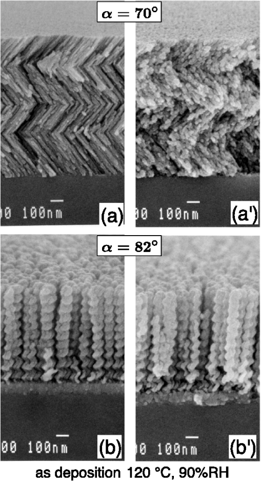
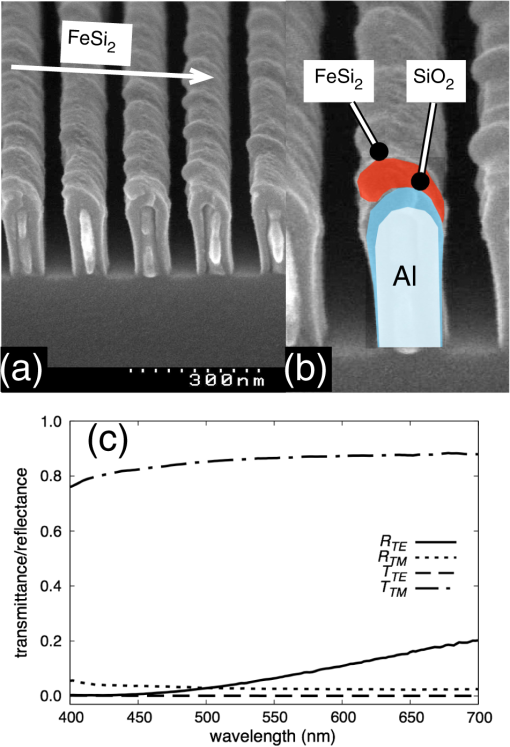
1.IntroductionThe excellent textbook authored by Lakhtakia and Messier1 teaches us that today’s major thin film deposition technologies, such as sputtering2 and thermal evaporation,3 originated in the middle of the 19th century. Since then, research and development on thin films has continued for more than 150 years. Today, thin film technologies have matured to the extent that thin films can be deposited over very large areas with excellent uniformity.4,5 In most recent practical thin films, functionalities originating from the materials’ own properties and uniformity, without internal structures larger than the nanometer scale, are well established. However, if we can control the internal nanomorphology in a well-reproducible manner, various useful properties might be added to the existing functionalities owing to the materials’ own properties. Although lithographic technologies are significantly developed, it is still difficult to form three-dimensional (3-D) nanomorphologies over large areas at low cost. On the other hand, one can self-assemble a 3-D nanomorphology by taking advantage of the thin film growth mechanism. One of the most powerful methods for controlling nanomorphology is oblique angle deposition (OAD) or glancing angle deposition (GLAD). Although the advanced functionalities of OAD films are well understood in academia, there seems to be prejudice in the industry that OAD thin films are neither durable nor reproducible. However, in the past few years, very fortunately, new products produced by the OAD technique have appeared on the market, including a substrate for surface-enhanced Raman spectroscopy6–8 and a low-reflectivity wire-grid polarizer.9,10 In this article, we discuss the practicability of OAD thin films and examples of the products produced by the OAD technique. 2.Example of OAD Thin Films and their Growth MechanismAbout 30 years after the major physical vapor deposition (PVD) techniques were developed, Kundt11 had already published the first report on OAD thin films.1 Because of the significant development of transmission electron microscopy (TEM), OAD thin films were investigated intensively during the 1960s. At present, research in this field is in its second century. Many of the active investigations on OAD thin films in the past two decades originated after the development of chevron- and helix-shaped columns by Motohiro and Taga12 and Robbie et al.,13 respectively. Here, we briefly introduce examples of OAD thin films (Fig. 1).8,14–16 During conventional PVD, the vapor is deposited on a substrate from the normal direction in vacuum so that flat, uniform thin films are produced. In contrast, during OAD, the substrate is set obliquely and sometimes rotated in-plane, as shown in Fig. 1(g). If the substrate temperature is sufficiently low, unique nanocolumnar structures such as zigzags, helixes, posts, and complex hybrid structures are created [Fig. 1(a)–1(e)]. Fig. 1Download(a)–(f) Typical examples of the nanocolumnar structures of OAD thin films8,14–16, and (g) a schematic drawing of the deposition geometry. 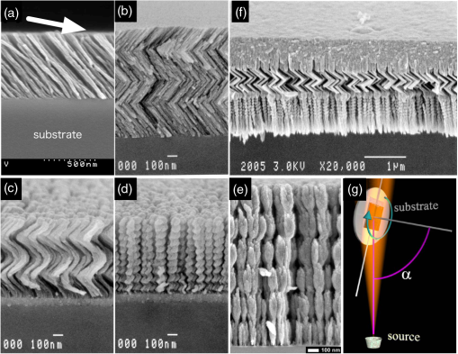 The physical origins of the columnar structure in OAD thin films are self-shadowing effects and the limited mobility of the deposited atoms. When the vapor flux is obliquely incident on the substrate surface, atoms in the growing films shadow unoccupied sites from the direct sticking of incident atoms [“shadowing effect,” Fig. 2(a)]. Moreover, owing to limited mobility, the unoccupied sites are not filled later [Fig. 2(b)]. As a result, oblique columns grow in the direction of the incident vapor beam [Fig. 2(c)]. The growth direction can be varied by changing the incident direction of the vapor flux. Fig. 2DownloadSchematic illustrations of the growth mechanism of the nanocolumnar structures: (a) nucleation, (b) onset of self-shadowing, and (c) nanocolumnar growth.  From the viewpoint of nanomorphological control, significant progress has been made in precise control17,18 and integration of shapes.16,19,20 In addition, many novel phenomena, especially unusual crystal growth21,22 induced by OAD, have been discovered. Owing to these well-controlled nanocolumnar morphologies, it has been well known that OAD thin films show shape-related anisotropy such as birefringence,1,12,23,24 dichroism,25,26 and magnetic anisotropy.27–29 Various advanced properties of OAD thin films have also been reported.14,30–33 For example, large surface area and high porosity are quite useful for surface chemical reactions,14 biochemical sensors,32 gas sensors,33 etc. These properties are also very attractive for practical applications. However, only a few OAD thin film products are currently available. The most successful example is the video tape.29 Other than the video tape, metal polarizers34,35 and birefringent coatings12,36 are also available. Apart from these examples, few products have been produced using the OAD technique. Most companies seem hesitant to introduce OAD into the factory. We believe that this is due to skepticism about the durability and reproducibility of OAD thin films. Thus, in the next section, we discuss the practicability of OAD thin films. 3.Practicability of OAD Thin FilmsWhen new materials are considered for introduction into practical devices, one requires functionality, productivity, and reliability. In the case of OAD thin films, many unusual and useful properties are available. Thus, let us consider the practicability of OAD thin films that have useful functionalities. 3.1.Productivity of OAD Thin FilmsMany researchers and engineers ask, “Can OAD thin films be mass-produced?” The answer is “Yes.” Many optical coatings are produced in a batch-type coater. Inside the deposition chamber, there are some evaporation sources and a large (typically 2 m in diameter) dome-shaped substrate holder. Such a substrate holder can carry hundreds of substrates. If the substrate holder is slightly modified, mounting the substrates obliquely and using planetary rotation are possible. Therefore, it is neither difficult nor very expensive to modify the standard coater for mass production of OAD thin films. However, unfortunately, we cannot avoid the decrease in the deposition rate. For example, at a deposition angle of 70 deg, the deposition rate becomes of the normal deposition rate. This might lead to slightly high cost for OAD films. However, by inputting slightly higher power to the deposition source, one can compensate for the decrease in the deposition rate. Consequently, mass production of OAD thin films is not a severe problem for practical applications. 3.2.Reliability of OAD Thin FilmsMany people who consider application of OAD thin films worry about their reliability. However, many, although not all, OAD thin films have sufficient reliability. For example, Fig. 3 shows photographs of a waveplate deposited in 199836 and kept in ambient conditions in the author’s office for more than 10 years. This film was deposited by using the Motohiro-Taga process12 at a deposition angle of 70 deg and has a chevron-shaped columnar cross-section. As indicated in Fig. 3(a), the film is completely transparent. From the photograph taken through polarizers shown in Fig. 3(b), it is clear that the retardation properties are quite uniform. Therefore, the film is very durable and exhibits high uniformity over . In addition, such a film is well reproducible because it was prepared by physical processes. Fig. 3DownloadVisual appearance of a waveplate of an OAD thin film36 taken (a) without and (b) with commercial sheet polarizers. 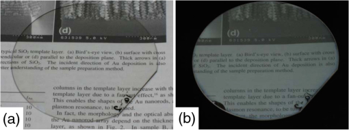 Another example is shown in Fig. 4. Generally, porous thin films are fragile. However, in many applications of thin films, the surface of the film is protected by a package or passivation coating. Users do not touch the surface of the OAD thin films in many cases. Remarkably, under some severe conditions, films with isolated columns are more stable than dense films. The scanning electron microscopy (SEM) images in Fig. 4(a’) and 4(b’) are those of columnar thin films processed under high-temperature air and water vapor.37 For the thin films with closely distributed columns, the columnar structure is destroyed by exposure to hot water vapor [Fig. 4(a’)]. In contrast, the thin films with isolated columns show no significant change in their morphologies [Fig. 4(b’)]. Therefore, the durability of OAD thin films is sufficient for appropriate applications. 3.3.DesignabilityManufacturers are extremely wary of production problems from unknown causes. Therefore, they often ask us, “Is the growth mechanism fully understood?” The answer may be, “Not fully, but sufficient to design the deposition process.” The complex shapes in OAD thin films can be reproduced by numerical simulations.15,38 The model is rather simple; that is, the deposition process is ballistic. Surface diffusion of the particles sticking to the surface is modeled by random walks. By using a Monte Carlo simulation based on this simple model, morphologies of the OAD films can be well reproduced. Monte Carlo simulations are also useful for designing film properties. Figure 5 indicates the results of work on developing Si rugate filters.15 If the deposition angle is changed during the deposition, the density can be changed continuously. When the deposition angle is large, the density becomes low and vice versa. Thus, we can control the refractive index continuously and create rugate optical filters by using only a single material. Fig. 5Download(a) SEM image of a Si rugate filter prepared based on the process designed by simulation, (b) the cross-sectional morphology of a simulated film, (c) depth profile of the packing density of the simulated film, and (d) comparison between the transmittance spectra of simulated and measured films.15 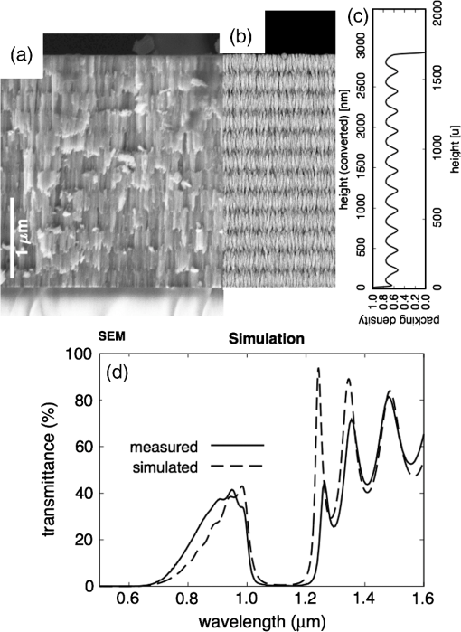 After some preliminary experiments, we prepared Si optical filters based on the process designed by Monte Carlo simulation. Figure 5(b) shows the cross-section of the designed film, and Fig. 5(a) shows a SEM image of the real film. The results, including the absolute film thickness, agree well with each other. Figure 5(d) displays the measured and designed transmittance spectra. Agreement between the measurement and design is excellent. Hence, the structure and properties of OAD films can be designed. OAD thin films thus have many advantages from the viewpoint of their functionality, while their weak points do not pose severe problems for practical applications. Therefore, if the prejudice on the part of manufacturers is removed, more OAD thin films can be expected to enter the market. In fact, we have succeeded in introducing new OAD products into the market by discussing these points with our collaborators in manufacturers. 4.Examples of Recent Practical Applications4.1.Au Nanorod Arrays for Surface-Enhanced Raman ScatteringMuch attention has been devoted to surface-enhanced Raman scattering (SERS) in the near-IR (NIR) region from the viewpoint of applications to biochemical sensors. SERS is a direct and very sensitive method for identifying molecules. It is well known that the local electric field enhanced by the plasma resonance in metal nanoparticles plays an important role in the strong enhancement of Raman scattering. For application to biological materials, the excitation in the NIR region is appropriate because this region is compatible with biological tissues’ transparency window.39 To develop NIR SERS substrates, the control of size, shape, and arrangement of nanoparticles is important. Elongated nanoparticles (so-called nanorods) are strong candidates for NIR SERS substrates because the local field can be significantly enhanced at their ends. Sensitive SERS properties of lithographically produced nanorod arrays have been reported.40,41 However, the high cost of these top-down processes has not yet been overcome. Although chemically produced nanorods also have tunable and very uniform shapes,42 they get distributed randomly on the substrate. As a result, not all nanorods align end to end, where further enhancement of the local field is expected. Nanorods created by simple OAD align side by side.43 However, we have succeeded in aligning the nanorods end to end by using OAD.44 Figure 6(a) shows the morphology of our Au nanorod arrays. Au nanorods were aligned on a template layer (called the “shape control layer”) having an anisotropic surface morphology prepared by OAD.6 The shape control layer of as the template for Au nanorods is prepared by a serial bideposition (SBD) technique. The glass substrate is set obliquely at a deposition angle of about 80 deg. During deposition, the substrate is rotated in-plane by 180 deg with each deposition of 10 nm of . As a result, the surface of the shape control layer prepared by SBD is corrugated anisotropically.6,7 On the anisotropic shape control layer, Au is also evaporated obliquely in vacuum. The amount of deposited Au is only around 10 nm thick on average. The Au sticks only to the top of the columns, owing to shadowing, and forms elongated nanoparticles (nanorods). Excellent SERS properties are observed, as indicated in Fig. 6(b), when the Raman spectra are measured on the Au nanorod arrays immersed in a solution of 4,4’-bipyridine.6 The SERS spectra can be detected down to of solution within a few minutes after the immersion of samples. In our measurement system, the spot size of the laser is around . The thickness of the nanorod array is of the order of 10 nm. Therefore, at , the number of molecules existing inside the SERS active volume is estimated to be fewer than 10 molecules. Thus, our nanorod arrays have a detection sensitivity of nearly a single molecule. The high sensitivity can be attributed to the high number density of nanorods and effective field concentration between in-line aligned nanorods. Fig. 6Download(a) SEM image of a Au nanorod array prepared on the OAD template layer and (b) the SERS spectra measured on a Au nanorod array in a solution of 4,4’-bipyridine.6 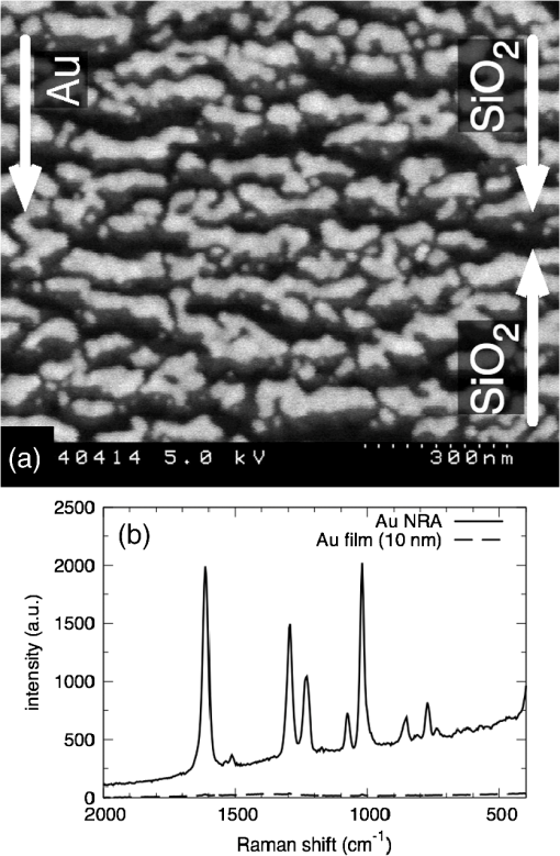 In addition to the high sensitivity, our nanorod arrays are well reproducible, and no contamination occurs during deposition. Moreover, they maintained high SERS sensitivity for more than one year.6 These are the advantages of the OAD technique. Fortunately, a Japanese coating company recently began to produce our nanorod arrays. These are already available on the market today. 4.2.Low-Reflectivity Wire-Grid PolarizersRecent liquid-crystal (LC) projectors require high thermal durability for their optical elements. Metal wire-grid (WG) polarizers are quite suitable because they are not degraded by heat and light.45 In addition, high reflectivity of the wire-grid polarizers is useful for recycling the light near the light source. However, highly reflective polarizers downstream might generate stray light, which might degrade image quality. Therefore, polymer sheet polarizers have been used in projectors and their durability significantly influences the lifetime of the total system. Thus, improving the brightness and durability of projectors requires the development of low-reflectivity (LR) WG polarizers. In other words, antireflective (AR) coatings for nanostructured metals are needed. From considerations based on optical admittance, we found that antireflectivity is always possible if we fabricate a multilayered thin film of absorptive and dielectric materials on a highly reflective metal.9 This bilayered AR concept has been applied to reduce the reflectance of WG polarizers made of Al. At first, we prepare aluminum WG polarizers by interference lithography and dry etching. The dielectric layer of is deposited by ordinary sputtering. The absorptive layer of is then deposited by ion beam sputtering at a glancing deposition angle of 87 deg from the surface normal. Because of the shadowing effect, the sputtered FeSi adheres only to the top of the WGs covered with . Figure 7(a) and 7(b)shows SEM images of an LR-WG polarizer.9 The thicknesses of and are 10 and 24 nm, respectively. The wires show bulges growing toward the incident direction of . This suggests that the bulges correspond to nanoparticles of deposited . Thus, it is expected that elongated nanoparticles are arrayed on the Al WG covered with the dielectric layer of . Similar structures can be fabricated, in principle, by conventional top-down processes. However, etching multilayers consisting of materials with very different properties is not easy, whereas OAD is robust in terms of selection of materials. In addition, the fact that conventional WG polarizers can be converted to LR-WG polarizers by simply depositing and is useful. Figure 7(c) indicates the reflectance and transmittance spectra of an LR-WG polarizer. Clearly, the reflectance of both TE and TM waves is very small. No significant degradation of the transmission properties is recognized. The extinction ratio of the LR-WG polarizers is slightly higher than the conventional WG polarizers and reaches 1500 to 2000.10 Because LR-WG polarizers are completely composed of inorganic materials, they are much more durable than polymer polarizers. The durability of the LR-WG pilarizers is basically identical to that of the conventional WG polarizers.45 Our LR-WG polarizers are now used in commercial LC projection displays that require high thermal durability. 5.SummaryWe reviewed the recent status of practical applications of OAD thin films. To remove the skepticism and prejudice of manufacturers, the practicability of OAD thin films was discussed. There are no significant problems in their production, reliability, and designability, which are important considerations for practical applications. In addition, we introduced two examples of our recent practical applications: Au nanorod arrays for SERS and low-reflectivity wire-grid polarizers. Both products are currently available on the market. AcknowledgmentsThis article has been prepared in collaboration with Kenji Kimura, Kaoru Nakajima, all members of the Nanomaterials Engineering Laboratory at Kyoto University, and Yasunori Yaga at Chubu University, Japan. Student contributions were especially important for carrying out the investigations. I am also grateful to Sadamu Kinoshita of Kyoto University for the SEM observations. This work was supported by KAKENHI 21656058 and 17310073. ReferencesA. LakhtakiaR. Messier, Sculptured Thin Films: Nanoengineered Morphology and Optics, 28
–48 SPIE, Bellingham
(2005). Google Scholar
W. R. Grove,
“On the electro-chemical polarity of gases,”
Phil. Trans. R. Soc. Lond., 142 87
–101
(1852). http://dx.doi.org/10.1098/rstl.1852.0008 PTRSAV 0370-2316 Google Scholar
M. Faraday,
“Experimental relations of gold (and other metals) to light,”
Phil. Trans. R. Soc. Lond., 147 145
–181
(1857). http://dx.doi.org/10.1098/rstl.1857.0011 PTRSAV 0370-2316 Google Scholar
D. M. Mattox, The Foundations of Vacuum Coating Technology, 24 William Andrew Publishing, New York
(2003). Google Scholar
K. S. Harsha, Principles of Vapor Deposition of Thin Films, 90 Elsevier Science, The Netherlands
(2006). Google Scholar
M. Suzukiet al.,
“Au nanorod arrays tailored for surface-enhanced Raman spectroscopy,”
Anal. Sci., 23
(7), 829
(2007). http://dx.doi.org/10.2116/analsci.23.829 ANSCEN 0910-6340 Google Scholar
M. Suzukiet al.,
“In-line aligned and bottom-up Ag nanorods for surface-enhanced Raman spectroscopy,”
Appl. Phys. Lett., 88
(20), 203121
(2006). http://dx.doi.org/10.1063/1.2205149 APPLAB 0003-6951 Google Scholar
M. Suzukiet al.,
“Ag nanorod arrays tailored for surface-enhanced Raman imaging in the near-infrared region,”
Nanotechnology, 19
(26), 265304
(2008). http://dx.doi.org/10.1088/0957-4484/19/26/265304 NNOTER 0957-4484 Google Scholar
M. Suzukiet al.,
“Antireflection coatings with FeSi2 layer: application to low-reflectivity wire grid polarizers,”
Thin Solid Films, 519
(24), 8485
–8489
(2011). http://dx.doi.org/10.1016/j.tsf.2011.05.023 THSFAP 0040-6090 Google Scholar
M. Suzukiet al.,
“Low-reflectivity wire-grid polarizers multilayered by the glancing-angle-deposition technique,”
J. Nanophoton., 5
(1), 011501
(2011). http://dx.doi.org/10.1117/1.3543821 JNOACQ 1934-2608 Google Scholar
A. Kundt,
“Ueber doppelbrechung des lichtes in metallschichten, welche durch zerstuben einer kathode hergestellt sind,”
Ann. Phys. (Berlin), 263
(1), 59
–71
(1886). http://dx.doi.org/10.1002/(ISSN)1521-3889 ANPYA2 0003-3804 Google Scholar
T. MotohiroY. Taga,
“Thin film retardation plate by oblique deposition,”
Appl. Opt., 28
(13), 2466
–2482
(1989). http://dx.doi.org/10.1364/AO.28.002466 APOPAI 0003-6935 Google Scholar
K. RobbieM. J. BrettA. Lakhtakia,
“Chiral sculptured thin films,”
Nature, 384
(6610), 616
(1996). http://dx.doi.org/10.1038/384616a0 NATUAS 0028-0836 Google Scholar
M. SuzukiT. ItoY. Taga,
“Photocatalysis of sculptured thin films of ,”
Appl. Phys. Lett., 78
(25), 3968
–3970
(2001). http://dx.doi.org/10.1063/1.1380730 APPLAB 0003-6951 Google Scholar
K. Kaminskaet al.,
“Simulating structure and optical response of vacuum evaporated porous rugate filters,”
J. Appl. Phys., 95
(6), 3055
–3062
(2004). http://dx.doi.org/10.1063/1.1649804 JAPIAU 0021-8979 Google Scholar
M. SuzukiY. Taga,
“Integrated sculptured thin films,”
Jpn. J. Appl. Phys., 40
(4A), L358
–L359
(2001). http://dx.doi.org/10.1143/JJAP.40.L358 JJAPA5 0021-4922 Google Scholar
B. Dicket al.,
“Periodic magnetic microstructures by glancing angle deposition,”
J. Vac. Sci. Technol. A, 18
(4), 1838
–1844
(2000). http://dx.doi.org/10.1116/1.582481 JVTAD6 0734-2101 Google Scholar
D. Yeet al.,
“Growth of uniformly aligned nanorod arrays by oblique angle deposition with two-phase substrate rotation,”
Nanotechnology, 15
(7), 817
–821
(2004). http://dx.doi.org/10.1088/0957-4484/15/7/018 NNOTER 0957-4484 Google Scholar
K. RobbieM. J. Brett,
“Sculptured thinfilms and glancing angle deposition: growth mechanics and applications,”
J. Vac. Sci. Technol. A, 15
(3), 1460
–1465
(1997). http://dx.doi.org/10.1116/1.580562 JVTAD6 0734-2101 Google Scholar
K. RobbieJ. C. SitM. J. Brett,
“Advanced techniques for glancing angle deposition,”
J. Vac. Sci. Technol. B, 16
(3), 1115
–1122
(1998). http://dx.doi.org/10.1116/1.590019 JVTBD9 0734-211X Google Scholar
T. Karabacaket al.,
“Beta-phase tungsten nanorod formation by oblique-angle sputter deposition,”
Appl. Phys. Lett., 83
(15), 3096
–3098
(2003). http://dx.doi.org/10.1063/1.1618944 APPLAB 0003-6951 Google Scholar
M. Suzukiet al.,
“Vapor phase growth of Al whiskers induced by glancing angle deposition at high temperature,”
Appl. Phys. Lett., 89
(13), 133103
(2006). http://dx.doi.org/10.1063/1.2357582 APPLAB 0003-6951 Google Scholar
H. A. Macleod,
“Structure-related optical properties of thin films,”
J. Vac. Sci. Technol. A, 4
(3), 418
–422
(1986). http://dx.doi.org/10.1116/1.573894 JVTAD6 0734-2101 Google Scholar
I. J. HodgkinsonQ. Wu, Birefringent Thin Films and Polarizing Elements, 1
–8 World Scientific, Singapore
(1997). Google Scholar
G. B. Smith,
“Theory of angular selective transmittance in oblique columnar thin films containing metal and voids,”
Appl. Opt., 29
(25), 3685
–3693
(1990). http://dx.doi.org/10.1364/AO.29.003685 APOPAI 0003-6935 Google Scholar
M. SuzukiY. Taga,
“Anisotropy in the optical absorption of thin films with oblique columnar structure,”
J. Appl. Phys., 71
(6), 2848
–2854
(1992). http://dx.doi.org/10.1063/1.351368 JAPIAU 0021-8979 Google Scholar
S. B. LuitjensC. Lodder,
“Metal evaporated tape; state of the art and prospects,”
J. Magn. Magn. Mater., 155
(1–3), 261
–265
(1996). http://dx.doi.org/10.1016/0304-8853(95)00727-X JMMMDC 0304-8853 Google Scholar
E. W. Pughet al.,
“Magnetic anisotropy in evaporated iron films,”
J. Appl. Phys., 31
(5), S293
(1960). http://dx.doi.org/10.1063/1.1984706 JAPIAU 0021-8979 Google Scholar
R. Sugita,
“Co-Cr perpendicular magnetic recording tape by vacuum deposition,”
IEEE. Trans. Magn., 20
(5), 687
–692
(1984). http://dx.doi.org/10.1109/TMAG.1984.1063204 IEMGAQ 0018-9464 Google Scholar
A. Lakhtakiaet al.,
“Sculptured thin films (STFs) for optical, chemical and biological applications,”
Innov. Mater. Res., 1
(2), 165
–176
(1996). IMREF4 0218-7566 Google Scholar
R. MessierA. Lakhtakia,
“Sculptured thin films –II. Experiments and applications,”
Mater. Res. Innovat., 2
(4), 217
–222
(1999). http://dx.doi.org/10.1007/s100190050088 MRINFV 1432-8917 Google Scholar
J. L. Martíneset al.,
“Anisotropic surface-enhanced Raman scattering at obliquely evaporated Ag films,”
Phys. Rev. B, 35
(18), 9481
–9488
(1987). http://dx.doi.org/10.1103/PhysRevB.35.9481 PRBMDO 0163-1829 Google Scholar
J. J. Steeleet al.,
“Impact of morphology on high-speed humidity sensor performance,”
IEEE Sensors J., 6
(1), 24
–27
(2006). http://dx.doi.org/10.1109/JSEN.2005.859359 ISJEAZ 1530-437X Google Scholar
R. E. Slocum,
“Evaporative thin metal films as polarizers,”
Proc. SPIE, 307 25
–30
(1981). http://dx.doi.org/10.1117/12.965901 PSISDG 0277-786X Google Scholar
R. E. SlocumD. Andrychuk,
“New near-infrared polarizers for laser applications,”
Proc. SPIE, 740 2
–7
(1987). http://dx.doi.org/10.1117/12.939726 PSISDG 0277-786X Google Scholar
M. SuzukiT. ItoY. Taga,
“Recent progress of obliquely deposited thin films for industrial applications (invited paper),”
Proc. SPIE, 3790 94
–105
(1999). http://dx.doi.org/10.1117/12.351241 PSISDG 0277-786X Google Scholar
M. SuzukiT. ItoY. Taga,
“Morphological stability of thin films with isolated columns,”
Jpn. J. Appl. Phys. Part 2, 40
(4A), L398
–L400
(2001). http://dx.doi.org/10.1143/JJAP.40.L398 JAPLD8 0021-4922 Google Scholar
M. SuzukiY. Taga,
“Numerical study of the effective surface area of obliquely deposited thin films,”
J. Appl. Phys., 90
(11), 5599
–5605
(2001). http://dx.doi.org/10.1063/1.1415534 JAPIAU 0021-8979 Google Scholar
B. Chance,
“Near-infrared images using continuous, phase-modulated, and pulsed light with quantitation of blood and blood oxygenation,”
Ann. NY Acad. Sci., 838 29
–45
(1998). http://dx.doi.org/10.1111/j.1749-6632.1998.tb08185.x ANYAA9 0077-8923 Google Scholar
P. F. Liaoet al.,
“Surface-enhanced Raman scattering from microlithographic silver particle surfaces,”
Chem. Phys. Lett., 82
(2), 355
–359
(1981). http://dx.doi.org/10.1016/0009-2614(81)85172-X CHPLBC 0009-2614 Google Scholar
G. Laurentet al.,
“Evidence of multipolar excitations in surface enhanced Raman scattering,”
Phys. Rev. B., 71
(4), 045430
(2005). http://dx.doi.org/10.1103/PhysRevB.71.045430 PRBMDO 1098-0121 Google Scholar
C. J. Orendorffet al.,
“Surface-enhanced Raman spectroscopy of self-assembled monolayers: Sandwich architecture and nanoparticle shape dependence,”
Anal. Chem., 77
(10), 3261
–3266
(2005). http://dx.doi.org/10.1021/ac048176x ANCHAM 0003-2700 Google Scholar
J. L. MartínesY. GaoT. López-Ríos,
“Surface-enhanced Raman scattering of obliquely evaporated Ag films,”
Phys. Rev. B., 33
(8), 5917
(1986). http://dx.doi.org/10.1103/PhysRevB.33.5917 PRBMDO 1098-0121 Google Scholar
M. Suzukiet al.,
“Direct formation of arrays of prolate Ag nanoparticles by dynamic oblique deposition,”
Jpn. J. Appl. Phys., 44
(5), L193
–L195
(2005). http://dx.doi.org/10.1143/JJAP.44.L193 JJAPA5 0021-4922 Google Scholar
D. Hansenet al.,
“The display applications and physics of the proflux wire grid polarizer,”
SID Int. Symp. Dig. Tech. Pap., 33
(1), 730
–733
(2002). http://dx.doi.org/10.1889/1.1830887 0097-966X Google Scholar
Biography Motofumi Suzuki is an associate professor at Kyoto University. He received his bachelor, master and doctor of engineering degrees from Kyoto University in 1986, 1988 and 1998, respectively. His current research interests include the optical properties of nanostructured thin films and the synthesis of novel nanostructures. He is a member of SPIE. |

