
|
|
1.IntroductionInGaAs cameras are commonly used to detect short-wavelength infrared (SWIR) light from 1 to 2 μm for night vision applications. However, the performance of typical InGaAs detectors decreases significantly in the ultraviolet (UV) and visible (Vis) spectral bands due to absorption of UV-Vis light in inactive regions of the detector. The ability to detect both the SWIR and UV with the same camera has application in flame identification for fire fighting, communications, muzzle flash identification, and covert tagging.1,2 We have previously reported the application of colloidal quantum dots (CQDs) to downshift UV light into the SWIR band to achieve efficient dual-band detection for a single-pixel InGaAs detector. A layer of CQDs deposited on the detector was shown to increase the average external quantum efficiency of the detector from 1.8 to 21% across the near UV from 300 to 400 nm.3 In this paper, we present three designs to incorporate CQDs into an InGaAs SWIR imaging system to create a UV-SWIR dual-band camera. In the first design, high-resolution dual-band imaging is realized using a new two-stage imaging camera and a CQD-based downshifting layer without modification of the InGaAs focal plane array (FPA). In the second design, the CQD-based downshifting layer is deposited directly on an SWIR-sensitive InGaAs FPA. A dramatic increase in the UV response with minimal change in sensitivity in the SWIR is observed. In the third design, the CQD downshifting layer is deposited on a substrate-thinned (ST) InGaAs FPA to achieve a high-resolution, multiband UV-Vis-SWIR camera. 2.Background2.1.InGaAs Focal Plane ArraysFigure 1(a) shows the design of a typical flip-chip InGaAs FPA mounted on silicon read-out integrated circuit (ROIC). The design is optimized to achieve a high external quantum efficiency across the SWIR spectral band. A layer of n-type InGaAs is grown on an InP substrate, and pixels are created by spatial patterning of p-type regions as depicted in red. Electrical contact between the ROIC and the FPA is made with indium bumps. The InGaAs FPA used in this paper is designed by Raytheon Vision Systems and consists of with a 20 μm pixel pitch. Fig. 1(a) Cartoon of flip-chip InGaAs FPA with InP substrate. SWIR light passes through the InP substrate and is collected in the active region of the pn junction. UV and visible light are absorbed in the InP substrate. (b) Cartoon of the CQD with semiconductor core surrounded by organic ligands. (c) Absorption (black line) and fluorescence (red line) spectra of 4.4 nm diameter PbS CQDs.  For InGaAs cameras with thick InP substrates, UV and visible light are collected in the InP substrate instead of in the active region of the InGaAs pn junction, as depicted in Fig. 1(a). To improve the UV-Vis performance, the InP substrate can be mechanically thinned. However, this increases the cost and performance in the UV is still poor. 2.2.Colloidal Quantum DotsCQDs are nanometer-sized semiconductor crystals synthesized using solution-based chemistry techniques.4 The crystalline core is surrounded by ligands that passivate the CQD surface and impart solubility as depicted in Fig. 1(b). Like bulk semiconductors, the CQDs absorb light with energy above the band gap and fluoresce near the band edge. However, due to quantum confinement in the CQD, the absorption and fluorescence wavelengths can be tuned by varying the size of the CQD core. The absorption and fluorescence spectra of the 4.4-nm diameter PbS CQDs used in this study are shown in Fig. 1(c).56.–7 The CQD size is chosen such that the emission is near the edge of the SWIR band. The brightness of the CQDs is characterized by the quantum yield (QY), the ratio of photons emitted to photons absorbed. For visible emitting CQDs, a QY of over 95% has been achieved.8 The QY of the SWIR emitting PbS CQDs used in this study is 45% in solution.3 By comparison, the best organic fluorophores emitting in this region have a QY of .9 2.3.Luminescent DownshiftingThe operation of the CQD-based luminescent downshifting (LDS) layer is depicted in Fig. 2(a).3 The CQD LDS layer is placed before the InGaAs detector and consists of a layer of CQDs embedded in polymethylmethacrylate (PMMA) deposited by spin coating. PMMA is a common, UV-SWIR transparent photoresist, which serves to disperse the CQDs. Fig. 2(a) Cartoon of the CQD LDS layer. The LDS layer is highly transparent to SWIR light. UV light is absorbed by the CQDs embedded in PMMA, downshifted, and emitted in the SWIR. (b) External quantum efficiency of a single-pixel detector before (black line) and after (red line) deposition of a CQD LDS layer. 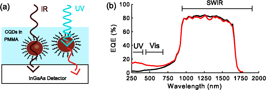 Since the CQDs absorb weakly in the SWIR compared to the UV, the LDS layer strongly absorbs incident UV light while remaining highly transparent to SWIR light. The absorbed light is downshifted and emitted in the SWIR band where it can be collected by the InGaAs detector. Ideally the CQDs are designed to emit at the short-wavelength edge of the SWIR band to reduce absorption in the SWIR region. Figure 2(b) shows the external quantum efficiency for a single-pixel InGaAs detector. The bare detector has minimal UV response. The red line in Fig. 2(b) shows the enhancement in UV response obtained with the addition of CQDs to downshift the incident light.3 Minimal loss of SWIR sensitivity is observed. 3.Results3.1.Design 1: Two-Stage CameraA two-stage camera has been designed to incorporate the CQD LDS layer without altering the InGaAs FPA [Fig. 3(a)]. In the first stage, a UV-SWIR transparent lens focuses the scene onto the LDS plate, which is positioned in the focal plane. Incident SWIR light is transmitted through the LDS plate and UV light is absorbed, downshifted, and emitted in the SWIR band by the CQDs. A second relay lens collects both the transmitted and downshifted SWIR light and focuses it on the InGaAs FPA. To demonstrate the effect of the LDS plate on the UV-Vis sensitivity of the camera, a series of filters are used such that only downshifted UV light is acquired by the InGaAs FPA, as depicted in Fig. 3(a). A short-pass filter (KG-3 Schott Glass) is used to filter out incident SWIR light and a long-pass filter (silicon) is used to block any UV-Vis light that passes through the LDS plate. We note that the long-pass filter is only used to test the performance of the LDS plate and is not necessary for operation of the camera. Fig. 3(a) Diagram of the two-stage dual-band camera. (b) Image taken using the two-stage camera. The subject is holding a UV light-emitting diode. A UV short-pass filter and IR long-pass filter are used such that only downshifted UV light is acquired. The inset shows the same image without the CQD LDS plate present. No image is observed. (c) Outdoor scene taken using the same settings as (b). 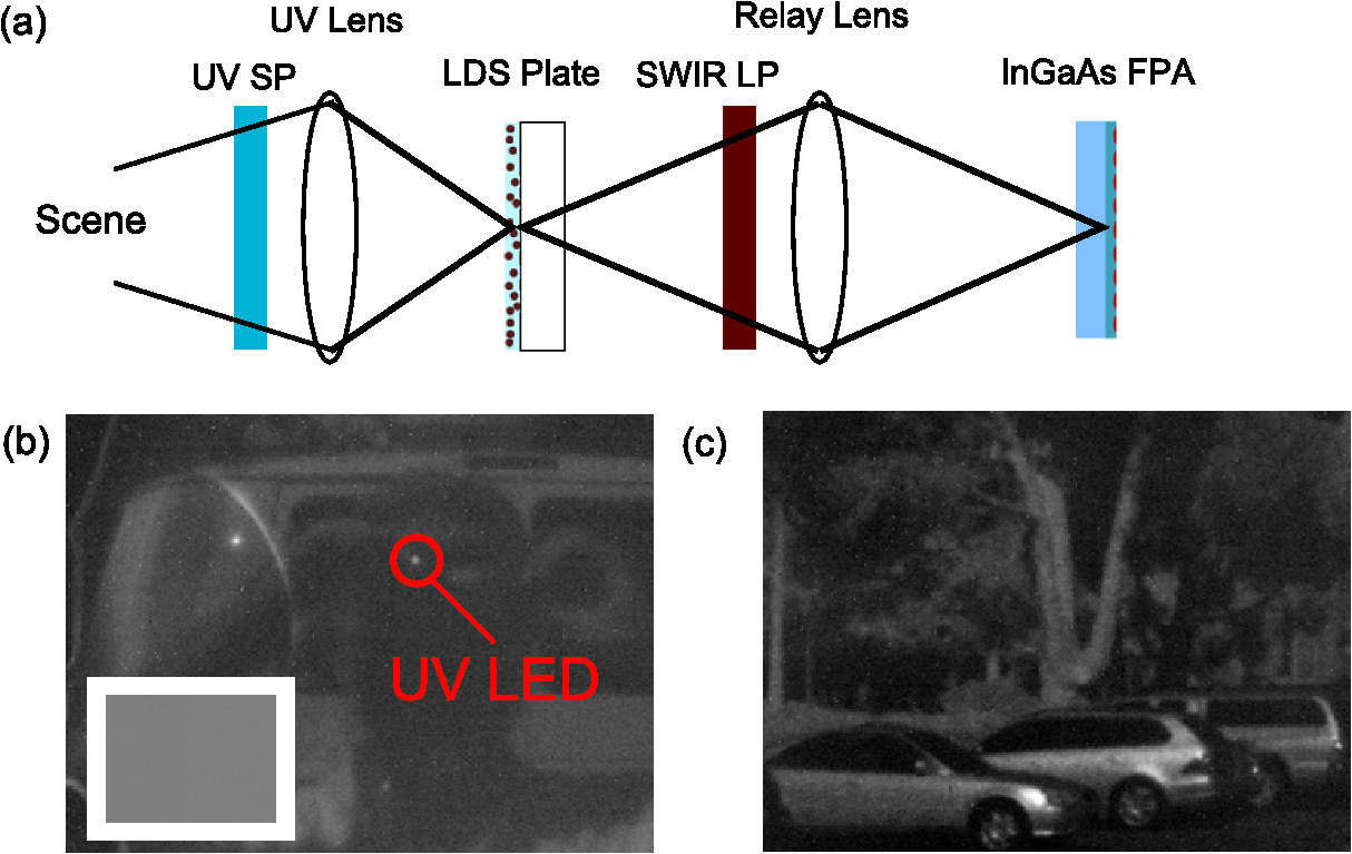 Figure 3(b) shows an image taken using the two-stage UV-SWIR camera and the LDS plate coated with PbS CQDs. Both the scene and the UV light-emitting diode (LED), held near eye level, are resolved by the camera system. The inset of Fig. 3(b) shows the response without the CQD plate present. No image is visible. Figure 3(c) shows an outdoor scene taken using the two-stage camera. Good contrast and high resolution are obtained. The advantage of this two-stage design is the ability to achieve dual-band imaging with a standard InGaAs camera. No permanent modification of the camera is required. The drawback of the two-stage design is that the downshifted light must be coupled out of the LDS layer into air, a transition from high to low index of refraction. A significant amount of reflection will occur at this interface, which will decrease the UV efficiency of the camera. This problem is solved in the next two camera designs. 3.2.Design 2: LDS Layer Deposited on FPAIn the second camera design, the LDS layer is directly deposited on the surface of the InGaAs array as depicted in Fig. 4(a). The InGaAs FPA is packaged and wire bonded prior to deposition. Without the CQD layer, the FPA is insensitive to UV light, as demonstrated by Fig. 4(b). After the LDS layer is deposited by spin coating, the UV sensitivity dramatically increases while the SWIR resolution and response remain largely unaffected as shown in Fig. 4(c). No damage to the wire bonds was observed after spin coating. Fig. 4(a) Cartoon of InGaAs FPA with CQD LDS layer deposited on the surface. (b) Image of a mug and a 400 nm emitting LED taken with the InGaAs FPA before deposition of the LDS layer. A KG-3 UV-Vis pass filter is placed in front of the LED to block any SWIR light emitted by the LED. (c) Same scene as (b) imaged after deposition of the LDS layer on the surface of the InGaAs FPA. A large increase in UV response is observed without significant degradation of SWIR response. (d) A false, two-color image of the scene taken with the LDS-enhanced InGaAs FPA. Green corresponds to an image under IR illumination with the LED off. Blue corresponds to an image of the same scene with the LED on and a KG-3 UV-Vis pass filter used to block the SWIR band. The blue LED response is much larger than the physical size of the UV LED (red circle) due to chromatic aberration. 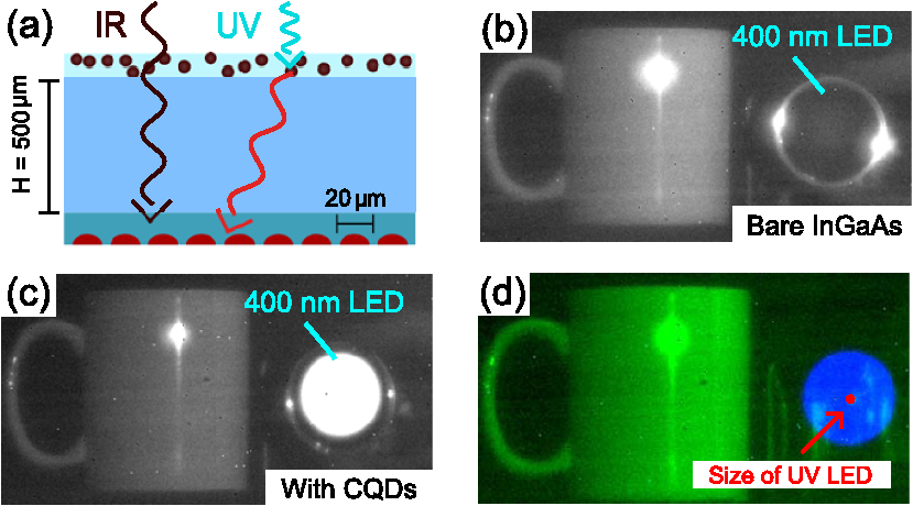 Figure 4(d) shows a false color image made from an image taken with the SWIR illumination off in blue and an image taken with the UV diode off in green. The approximate physical size of the UV LED is depicted by the red circle in Fig. 4(d). The measured UV response has a significantly larger apparent size than the physical size of the UV LED. This is a result of a decrease in the UV resolution of the imaging system. The loss of UV resolution is due to a combination of two effects: chromatic aberration due to the lens and optical cross-talk due to the LDS layer and the thick InP substrate. Figure 5(a) depicts the effect of chromatic aberration on the resolution. Since the index of refraction of the lens changes with wavelength, the focal length is significantly different in the UV and SWIR regions. Figures 5(b) and 5(c) shows the same image with the SWIR in focus and the UV in focus, respectively. Figures 5(b) and 5(c) is combined in a false color image in Fig. 5(d). Comparing the blue (UV focused) and green (SWIR focused) channels in Fig. 5(d), a significant difference in the UV LED spot size and position under SWIR focus due to chromatic aberration is observed. Chromatic aberration can be removed by using an achromatic lens such as the CoastalOpt UV-Vis-IR 60 mm lens. Although chromatic aberration is generally a negative aspect of a lens, we note that taking sequential images of the scene with the SWIR and then the UV in focus provides a method to achieve spectrally resolved false color images without filters. This is demonstrated in Fig. 5(d). Fig. 5(a) Cartoon depicting the effect of chromatic aberration on the resolution of UV light when the SWIR image is in focus. (b) Image of a hand and an LED power supply taken with a CQD-coated InGaAs FPA. The scene is illuminated with SWIR light. Light from a 285 nm LED is spread out in a large circle on the focal plane due to chromatic aberration. (c) The same scene with the 285 nm LED in focus. (d) False color comparison of (b) in green and (c) in blue showing the use of chromatic aberration to achieve spectral resolution.  The second contribution to the loss of UV resolution is due to the thick InP substrate and the emission pattern of the downshifted light. As depicted in Fig. 4(a), SWIR light is not absorbed by the LDS layer and is collected with no loss in resolution. UV light is absorbed, downshifted, and re-emitted. Since the InP substrate height, , is thick relative to the pixel size of 20 μm, the downshifted photons may travel a significant lateral distance from the point of absorption prior to striking the InGaAs pixels. Figure 6(a) shows an image of a mug under UV illumination collected with the CQD-coated FPA. The image is in focus, but the resolution is poor. Fig. 6(a) Image of a mug illuminated with 365 nm light taken with the CQD-coated InGaAs FPA. The image is in focus. The loss of resolution is due to the lateral distance traveled by the downshifted light in the 500 μm thick InP substrate. (b) Image of a 285 nm LED taken with the CQD-coated InGaAs FPA. For comparison, (c) shows the same image taken at high resolution with the bare, substrate-thinned (ST) detector discussed below. (d) The cross-section intensity profile (black line) from (c). The red line marks the position on the FPA that corresponds to the critical angle for total internal reflection.  To characterize the intrinsic UV resolution of the CQD-coated FPA, we measured the response to a 285 nm LED as shown in Fig. 6(b). For comparison, Fig. 6(c) shows the same image taken with the high-resolution, ST detector discussed below. For the CQD-coated FPA, a distinctive ring pattern is observed. Since the CQDs are in a thin film in between two different dielectric environments, it is not valid to assume isotropic emission of the downshifted light. The emission pattern of a fluorophore between two different dielectric interfaces is considered in detail by Lukosz.10,11 A peak in the emission starting at the critical angle for total internal reflection is predicted. This is observed in Fig. 6(d), which shows the cross-section of the ring pattern. The position on the FPA corresponding to the critical angle, , is given by Eq. (1). where is the thickness of the InP substrate, is the index of refraction of InP, and is the index of air. The calculated value for of 160 μm [red line in Fig. 6(d)] agrees with the observed position of the ring pattern.3.3.Design 3: LDS Layer on Substrate-Thinned FPAThe InP substrate of the InGaAs camera can be mechanically thinned to increase the sensitivity of the bare InGaAs FPA to UV and visible light, as depicted in Fig. 7(a). The improvement in UV-Vis performance of the bare ST InGaAs camera is demonstrated in Fig. 7(b). The scene is illuminated with visible light (no SWIR light). Both the mug and a 285 nm LED are imaged by the bare ST camera. Fig. 7(a) Cartoon of ST InGaAs FPA. (b) Image of a mug and 285 nm LED under visible illumination taken with the bare ST FPA. Inset: Image taken with 285 nm LED in focus showing UV response. (c) Image of a mug under SWIR illumination and a 285 nm LED taken with partially coated ST FPA. The red line marks the right edge of the LDS layer. An increase in the UV sensitivity to the left of the boundary due to the LDS layer is observed. (d) Image of an out-of-focus 285 nm LED taken with the bare ST FPA. (e) Same image taken with the LDS-coated ST FPA. A fivefold increase in the response is observed. 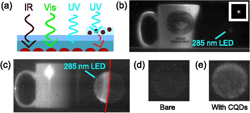 Figures 7(c)–7(e) demonstrates that the CQD LDS layer can be used to significantly improve the UV sensitivity above the state-of-the-art performance of the ST InGaAs camera. To accurately compare the response of the bare and LDS-coated ST FPA, only part of the FPA is coated with the LDS layer. Figure 7(c) shows an image of a mug and 285 nm LED under SWIR illumination. High resolution in the SWIR region is observed, as is the increase in the UV response due to the LDS layer. Figures 7(d) and 7(e) shows the response of the bare and the LDS-coated ST FPA, respectively, to an out-of-focus 285 nm LED. The response of the LDS-coated FPA is fivefold greater than the response of the bare ST FPA. To test the resolution of the CQD-coated ST FPA, we imaged two scenes under UV excitation. Figures 8(a)–8(c) shows a mug under 365 nm illumination. On the bare substrate-thinned FPA, a high-resolution image is obtained but the intensity of the response is low [Fig. 8(a)]. When the mug is imaged on the edge of the LDS layer as shown in Fig. 8(b), an increase in response due to the LDS layer is clear and the high resolution is maintained. Comparing Fig. 8(c) to the image in Fig. 6(a) taken with the thick substrate CQD-coated FPA demonstrates the effect of thinning the InP substrate on the resolution. Since the downshifted light travels a shorter lateral distance before striking the InGaAs pixels, as depicted in Fig. 7(a), no resolution loss in the UV is observed for the LDS-coated portion of the ST FPA. The lines across the mug in Fig. 8(c) are due to the nonuniformity of the drop cast film used to partially coat the FPA and would not be present in a higher-quality spin-coated film covering the entire array. Fig. 8Image of a mug under 365 nm excitation acquired on (a) bare ST FPA, (b) edge of LDS layer (red line), (c) middle of LDS layer.  Video 1 is collected at 8 Hz with the CQD-coated portion of the ST FPA and shows a face illuminated with 365 nm light. The video demonstrates the high resolution obtainable in the UV with the ST FPA. Video 1The lower half of a face is illuminated with 365 nm light and the image is collected with the CQD-coated portion of the ST FPA. (Video 1, MOV, 0.5 MB) [URL: http://dx.doi.org/10.1117/1.JNP.7.1.073083.1].  4.ConclusionWe have demonstrated the application of CQDs to sensitize an InGaAs camera system to the UV region using three distinct camera designs. The dual lens design allows any SWIR camera to be temporarily modified to a dual-band imaging system. For applications that do not require high resolution in the UV, this design may be a good compromise between cost and performance. In the second design, depositing the LDS layer on a standard InGaAs FPA is a low-cost design to achieve efficient dual-band sensitivity. In the third design, we have shown that for applications where high-resolution UV imaging is required, the LDS layer can enhance the UV sensitivity of an ST InGaAs detector by fivefold while maintaining high UV resolution. The LDS layer extends the range of the ST FPA into the UV to create a state-of-the-art UV-Vis-SWIR multiband camera. AcknowledgmentsThe authors gratefully acknowledge the following: D. Acton, M. Weinberg, and C. Tracy for imaging setup; D. Knapp for optics design; J. Wyles and S. Tailor for technical discussions; and J. Getty for providing the FPA. This work was supported by the U.S. Army through the Institute for Soldier Nanotechnologies (W911NF-07-D-004). J. M. S. acknowledges the support of the Department of Defense through the National Defense Science and Engineering Graduate Fellowship program. S. M. G. wrote the manuscript, deposited the QDs, and participated in the imaging; J. M. S. synthesized and processed the QDs under the supervision of M. G. B.; M. D. J. contributed to the design of the dual-lens camera; and F. B. J. led the project and participated in the imaging. ReferencesG. Ariyawansaet al.,
“GaN/AlGaN ultraviolet/infrared dual-band detector,”
Appl. Phys. Lett., 89
(9), 091113
(2006). http://dx.doi.org/10.1063/1.2345226 APPLAB 0003-6951 Google Scholar
R. C. Jayasingheet al.,
“Simultaneous detection of ultraviolet and infrared radiation in a single GaN/GaAlN heterojunction,”
Opt. Lett., 33
(21), 2422
–2424
(2008). http://dx.doi.org/10.1364/OL.33.002422 OPLEDP 0146-9592 Google Scholar
S. M. Geyeret al.,
“Efficient luminescent down-shifting detectors based on colloidal quantum dots for dual-band detection applications,”
ACS Nano., 5
(7), 5566
–5571
(2011). http://dx.doi.org/10.1021/nn2010238 1936-0851 Google Scholar
C. B. MurrayC. R. KaganM. G. Bawendi,
“Synthesis and characterization of monodisperse nanocrystals and close-packed nanocrystal assemblies,”
Annu. Rev. Mater. Sci., 30
(1), 545
–610
(2000). http://dx.doi.org/10.1146/annurev.matsci.30.1.545 ARMSCX 0084-6600 Google Scholar
L. Cademartiriet al.,
“Size-dependent extinction coefficients of PbS quantum dots,”
J. Am. Chem. Soc., 128
(31), 10337
–10346
(2006). http://dx.doi.org/10.1021/ja063166u JACSAT 0002-7863 Google Scholar
M. A. HinesG. D. Scholes,
“Colloidal PbS nanocrystals with size-tunable near-infrared emission: observation of post-synthesis self-narrowing of the particle size distribution,”
Adv. Mater., 15
(21), 1844
–1849
(2003). http://dx.doi.org/10.1002/(ISSN)1521-4095 ADVMEW 0935-9648 Google Scholar
J. M. Pietrygaet al.,
“Utilizing the lability of lead selenide to produce heterostructured nanocrystals with bright, stable infrared emission,”
J. Am. Chem. Soc., 130
(14), 4879
–4885
(2008). http://dx.doi.org/10.1021/ja710437r JACSAT 0002-7863 Google Scholar
A. B. Greytaket al.,
“Alternating layer addition approach to cdse/cds core/shell quantum dots with near-unity quantum yield and high on-time fractions,”
Chem. Sci., 3 2028
–2034
(2012). http://dx.doi.org/10.1039/c2sc00561a CESCAC 0009-2509 Google Scholar
K. RurackM. Spieles,
“Fluorescence quantum yields of a series of red and near-infrared dyes emitting at 600–1000 nm,”
Anal. Chem., 83
(4), 1232
–1242
(2011). http://dx.doi.org/10.1021/ac101329h ANCHAM 0003-2700 Google Scholar
W. Lukosz,
“Light emission by magnetic and electric dipoles close to a plane dielectric interface. III. Radiation patterns of dipoles with arbitrary orientation,”
J. Opt. Soc. Am., 69
(11), 1495
–1503
(1979). http://dx.doi.org/10.1364/JOSA.69.001495 JOSAAH 0030-3941 Google Scholar
W. LukoszR. E. Kunz,
“Light emission by magnetic and electric dipoles close to a plane interface. I. Total radiated power,”
J. Opt. Soc. Am., 67
(12), 1607
–1615
(1977). http://dx.doi.org/10.1364/JOSA.67.001607 JOSAAH 0030-3941 Google Scholar
Biography Scott M. Geyer received his BSc degree in physical chemistry from the University of Virginia, Charlottesville, Virginia, in 2005 and his PhD degree in 2010 from the Massachusetts Institute of Technology (MIT), Cambridge, Massachusetts. His PhD research focused on optoelectronic applications of infrared quantum dots.  Jennifer M. Scherer received her BS degree in chemistry from The Ohio State University, Columbus, in 2009. She is currently pursuing her PhD degree in the Department of Chemistry at MIT, Cambridge, Massachusetts, with research focused on quantum dot optoelectronics.  Michael D. Jack received his PhD degree in solid-state physics from University of California, Berkeley. He is a senior Raytheon engineering fellow and technical director of HgCdTe Avalanche Photodiodes Products at Raytheon Vision Systems, Goleta, California. He is also currently responsible for technical direction and development of SWIR detectors for high dynamic range, high sensitivity, small-pixel SWIR imagers.  Moungi G. Bawendi received his AB degree in chemistry from Harvard University, Cambridge, in 1982, his AM degree from Harvard University, Cambridge, in 1983, and his PhD degree from the University of Chicago, Chicago, Illinois, in 1988. He is currently the Lester Wolfe professor of chemistry at MIT, Cambridge, Massachusetts.  Frank B. Jaworski received his PhD degree in physics from University of California, Irvine, and is a senior principal electrical engineer at Raytheon Vision Systems, Goleta, California. He is currently active in the development of very large format focal plane arrays and is the program manager at RVS, responsible for nanotechnology development with the Institute of Soldier Nanotechnology at MIT. |


