|
|
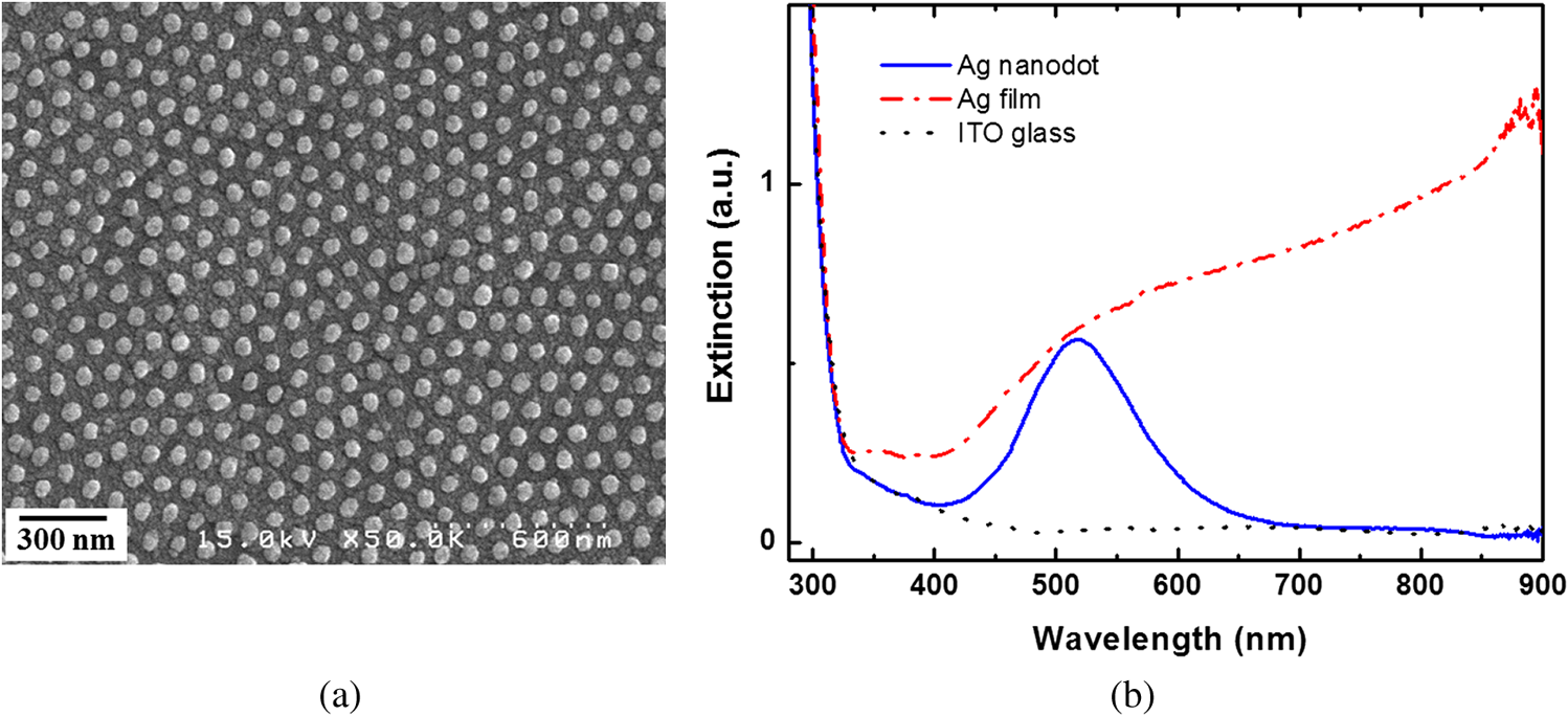
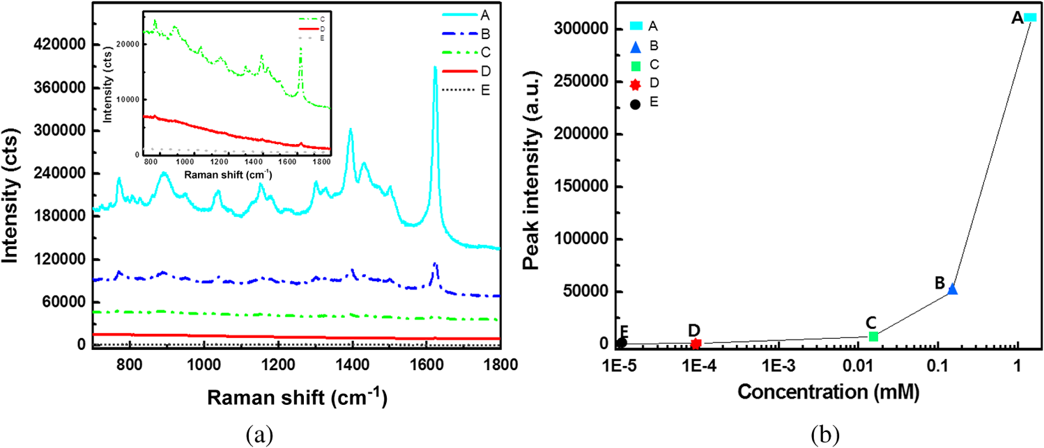
1.IntroductionSurface-enhanced Raman spectroscopy has attracted significant attention as an analytical technique for the sensitive and selective detection of molecules adsorbed on some roughened metal or nano-size metal surfaces.1,2 Surface-enhanced Raman scattering (SERS) is achieved based on the strong enhancement of its vibrational signals through the amplification of electromagnetic fields, and the fields are generated by the excitation of localized surface plasmon on a metal nanostructured surface.2 One of the primary topics for applications of SERS is to prepare an SERS-active surface. Many researchers have attempted to make SERS-active surfaces via diverse methods including chemical etching,3 island lithography chemical etching,4 and nanosphere lithography.5 Various metallic nanostructured surfaces, such as roughened silver electrode,6 gold nanostructured film,7 gold colloidal nanoparticles,8 cap-shaped silver nanoparticles,9 nanostructured gold-coated substrate,10 and gold nanopillar arrays,11 have been proposed for SERS-active substrates. The plasmonic properties are correlated with the metal nanostructured surface. In other words, the structure of the metal nanoparticles affects the enhancing capability of an SERS-active surface, and the capability is quantified by the quantity called enhancement factor.12 SERS enhancements rely on surface plasmon resonances associated with plasmonic phenomenon, in which conduction electrons oscillate coherently with the frequency of an applied radiation field.13 The metal nanostructures have potential applications as building blocks for highly sensitive biological and chemical sensors.13,14 The stability and reproducibility of SERS-active substrates are still the difficulties to be surmounted for practical applications.9 The fabrication of metal nanostructured surface with the stability and reproducibility is the main difficulty. Thus, the fabrication technique of noble metal nanostructured surface is a significant factor for performing SERS experiments. The technique used in this work is a nanofabrication method using nanoporous alumina template. The nanoporous alumina mask can be reproducibly obtained from a self-organized anodic aluminum oxide layer prepared by an anodization method. The structure of porous alumina layer is close-packed hexagonal columnar cell array containing a central pore normal to the aluminum substrate. The nanoporous alumina mask with through-holes was achieved by removing the barrier alumina layer on the aluminum. The fabrication technique of nanostructured surface using the nanoporous alumina mask has several advantages such as reproducibility, stability, and low cost. Many kinds of nanostructures including nanoholes,15 nanorods,16 and nanodots17–20 have been fabricated using nanoporous alumina masks. Particularly, the nanoporous alumina mask has been used as an evaporation mask to fabricate various nanodot arrays.17–21 So far, there has been intensive research on the fabrication of nanodot arrays on a substrate, but little effort has focused on the height of Au nanodots for maximizing the efficiency of SERS.21 The advantage of using the nanoporous alumina mask for the preparation of metal nanostructure for SERS is the controllability of the dimension of metal nanodot.21 In addition, the metal nanodot can be reproducibly prepared from the nanoporous alumina masks. In this study, we report the fabrication of Ag nanodot array on indium-tin-oxide (ITO) glass via alumina mask with through-holes and the utilization of this array as a substrate for SERS. Note that the ITO glass refers to ITO-coated glass with good transparency and conductivity. The reason for using ITO glass as a substrate instead of popular or BK-7 (metal-coated Pyrex 7740 glass) for surface plasmon resonance is because the focus of this experiment was to detect the Raman signal only from Ag nanodot array, not from substrate for sensitive detection. Any radiations from substrate were not desired, and BK-7 and simple glass radiate the undesired signals much more than that of ITO glass. The plasmonic property of Ag nanodot array on ITO glass was examined by UV spectroscopy. The SERS activity of Ag nanodot array on ITO glass was investigated by varying a concentration of methylene blue (MB) on Ag nanodot array, where MB is used as an SERS probe material. 2.Experiments2.1.Preparation of Nanoporous Alumina Mask and Ag Nanodot ArrayWell-ordered nanoporous alumina layer was prepared from an aluminum foil using two-step anodization process devised by Masuda and Satoh.17 The anodization step was performed by applying 40 V bias in a 0.3 M at 3°C. Very thin nanoporous alumina mask in large dimension was prepared by two-time wet chemical etching.18 After the second anodization, the aluminum oxide layer was slightly etched in 5 wt.% solution at 30°C. Subsequently, a protecting layer on the surface of the aluminum oxide layer was coated, and the remaining aluminum substrate was completely removed using saturated solution. Then, the aluminum oxide layer was dipped again in 5 wt.% solution. Finally, the protecting layer was dissolved in acetone and then rinsed in distilled water. The fabricated nanoporous alumina mask with through-holes was placed on the surface of the ITO glass substrate. The fabrication process of the alumina mask is well described in detail elsewhere.18 Silver was deposited onto the surface of ITO glass by electron beam evaporation that is masked by the nanoporous alumina mask with through-holes. Under the vacuum of , 50-nm thick film of silver was deposited via electron beam evaporation at a deposition rate of . After the deposition, the alumina mask was selectively dissolved in 1 M NaOH for several minutes. The Ag nanodot array was fabricated on the ITO glass substrate, which referred to as the Ag nanodot array/ITO glass. 2.2.Surface and Optical Characterization of Ag Nanodot ArrayThe morphologies of the nanoporous alumina mask and Ag nanodot array were characterized by field emission scanning electron microscopy (FESEM) (Hitach S-4700). The absorption spectrum of Ag nanodot array/ITO glass was measured by an ultraviolet–visible (UV–Vis) spectrometer (Perkin Elmer Lambda 18). The optical property of MB adsorption on Ag nanodot array/ITO glass was examined by Raman spectrometer (LabRAM HR). Raman measurements were made in backscattering geometry with a LabRam HR fitted with a liquid nitrogen–cooled CCD detector. The spectra were collected under ambient conditions using the 633-nm line of a laser. The power of the laser was adjusted from 0.1 to 2 mW according to the concentration of MB. 3.Results and Discussion3.1.Preparation of Ag Nanodot ArrayThe fabrication of Ag nanodot array/ITO glass begins with the preparation of the nanoporous alumina mask. The nanoporous alumina mask was fabricated from 99.999% pure aluminum foil. The structure of porous alumina layer is a self-organized close-packed hexagonal cell array containing a central pore on the aluminum substrate. The aluminum oxide layer was composed of a porous alumina layer containing a central pore and the bottom barrier alumina layer. The nanoporous alumina mask with through-holes was made by removing the bottom barrier alumina layer. The density of nanodot arrays/ITO glass can be controlled through the anodization condition of the alumina mask.19 The shape and size of the nanodot arrays can be adjusted by changing the aspect ratio of the alumina masks.20 The crucial issue in preparing the nanoporous alumina mask for its usage as an evaporation mask is the complete removal of the bottom barrier alumina layer. We prepared a very thin nanoporous alumina mask with through-holes using a two-step chemical wet etching process.18 The schematic illustrations of fabrication process and the FESEM images of Ag nanodot array/ITO glass are shown in Fig. 1. The FESEM image of ITO glass covered with the alumina mask is shown in Fig. 1(d). The thickness of the nanoporous alumina mask with through-holes was about 200 nm. After the second anodization for 4 min, the aluminum oxide layer was etched slightly for 12 min in 5 wt.% solution at 30°C. After dissolving the remaining aluminum substrate, the aluminum oxide layer was dipped again for 9 min in 5 wt.% solution. The nanoporous alumina mask was put on the surface of ITO glass. The pore diameter and the hexagonal cell size of the mask were 60 and 105 nm, respectively. After silver deposition, the FESEM image of the top surface of the alumina mask and Ag nanodot array/ITO glass is shown in Fig. 1(e). After the partial removal of the alumina mask by adhesion of carbon tape, there are metal clusters on the top surface of the residual alumina mask. Figure 1(f) shows well-arranged Ag nanodot array/ITO glass after completely removing the alumina mask. The uniform nanodot array/ITO glass was formed in periodic patterns with a mean separation of 105 nm. The average diameter of the nanodots was , which is the same as the pore size of the mask. The alumina mask attached on the ITO glass substrate mainly determines the distribution of the nanodot arrays. Fig. 1Schematic illustrations of preparation process of Ag nanodot array: (a) the nanoporous alumina mask, (b) Ag deposited on the nanoporous alumina mask, and (c) Ag nanodot array on indium-tin-oxide (ITO) glass after dissolving the alumina mask. Corresponding field emission scanning electron microscopy (FESEM) images of preparation process of Ag nanodot array: (d) the nanoporous alumina mask, (e) Ag deposited on the nanoporous alumina mask, and (f) Ag nanodot array on ITO glass. 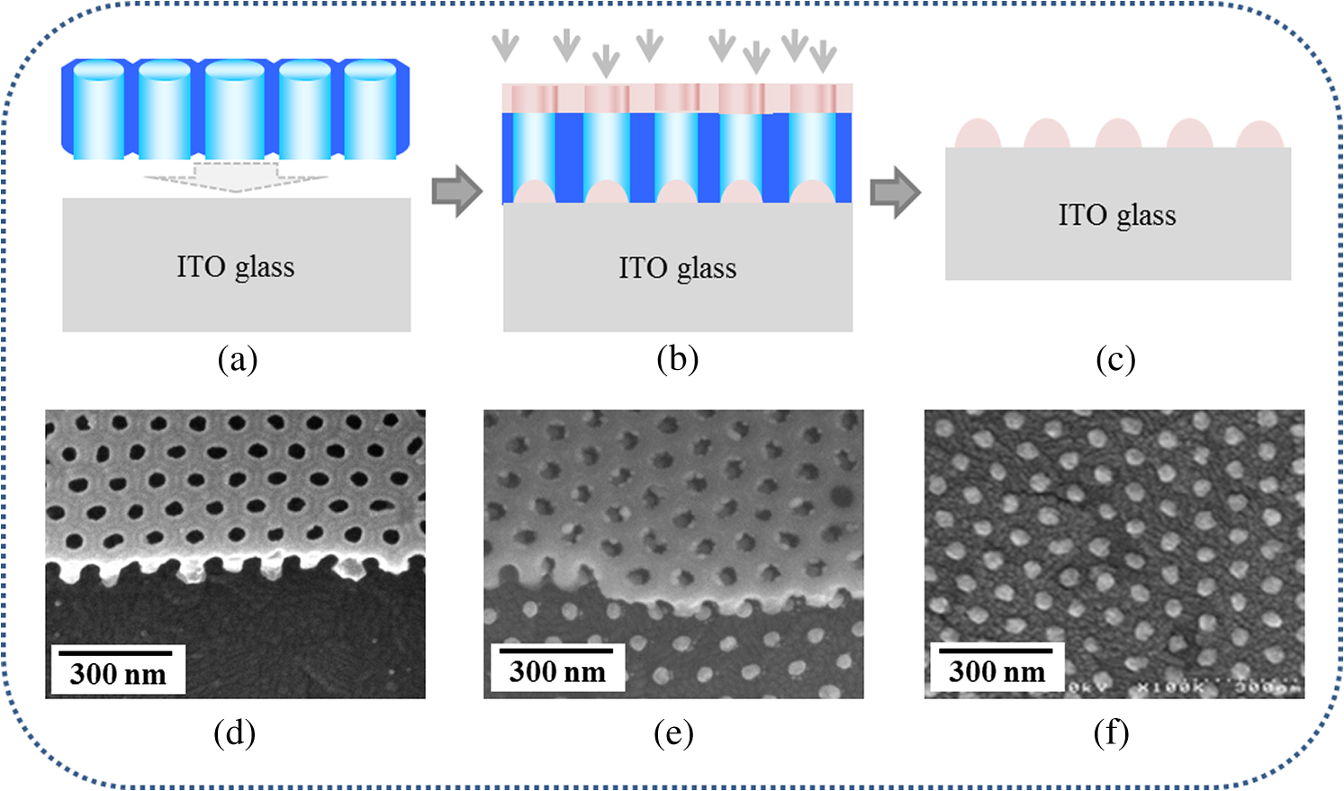 Localized surface plasmon resonance (LSPR) extinction for Ag nanodot array occurred near the maximum absorption wavelength of the electromagnetic wave. Because the excitation of LSPR on the metal nanostructured surface lies at the hard core of SERS,1 the fabrication technique of noble metal nanostructures is also a crucial factor for performing an SERS experiment. The plasmonic property of Ag nanodot array/ITO glass was examined by UV extinction spectroscopy. The typical FESEM image of Ag nanodot array/ITO glass shown in Fig. 2(a) and the extinction spectrum shown in Fig. 2(b) proves that a uniform and well-ordered Ag nanodot array was formed on the ITO glass. The UV spectrum for the Ag nanodot/ITO glass with the diameter of shows the maximum extinction peak at 518 nm. The extinction maximum depends on the composition, size, structure, and shape of the metal nanostructure.12 The LSPR is sensitive to the surrounding medium, so probing a change in refractive index can be used for monitoring adsorbates on the plasmonic particle.13 The sensitivity of the LSPR to the local environment can be utilized as a biochemical sensor by measuring wavelength shifts in extinction spectra.13 3.2.SERS Characterization of Ag Nanodot ArrayThe most important factor for performing an SERS experiment is to fabricate an SERS-active surface. The Raman enhancement is affected by the optical properties of a substrate. The effect of substrate for SERS-active surface was explored on three different SERS substrates, which were Ag nanodot array on ITO glass substrate, 50-nm thick Ag film on ITO glass substrate, and bare ITO glass substrate. In order to confirm the SERS effect, MB of 0.15 mM concentration, as SERS probe, was dispersed on those three different substrates. The Raman spectra from those three different samples with the same adsorption in the same concentration of MB are presented in Fig. 3. All the Raman spectra were recorded under the same measurement conditions by a laser with the wavelength of 633 nm and the power of 1 mW. As shown in Fig. 3, the Raman spectra obtained from those three samples are substantially different. The Raman spectrum from the bare ITO glass substrate was not observed under the measurement condition. The SERS signal from MB adsorbed on Ag nanodot array/ITO glass was dramatically enhanced compared with that on Ag film/ITO glass. Based on the Raman band of MB at , the Raman intensity from MB on the Ag nanodot array/ITO glass was increased about 40 times compared with that on Ag film/ITO glass, confirming the significant role of Ag nanodot array on the Raman signal enhancement. The Raman spectrum from MB adsorbed on Ag nanodot array/ITO glass is called SERS. The intensity of Raman signals from MB adsorbed on a commercial glass substrate was similar to that on Ag film/ITO glass. In order to achieve the lowest limits of SERS detection, we need to obtain the signals only from MB on the Ag nanodot array. To do so, we selected the ITO glass to minimize the effect from a glass substrate. These results revealed that the Ag nanodot array shows predominant effect in Raman scattering in terms of the signal intensity and spectral shape for SERS-active surface. Fig. 3Surface-enhanced Raman spectra (SERS) from methylene blue (MB) on different substrates: Ag nanodot array on ITO glass (solid line), 50-nm-thick Ag film on ITO glass (dash-dotted line), and ITO glass substrate (dotted line). The concentration of MB is 0.15 mM. 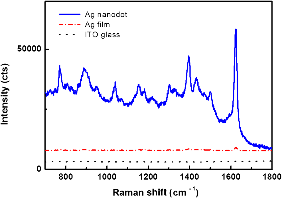 Figure 4 shows the SERS spectra from MB with concentration varying from 0.1 μM to 1.5 mM on the Ag nanodot array. The SERS intensities from Ag nanodot array/ITO glass were steadily increased with the concentration of MB. The SERS intensity from the 1.5 mM concentration of MB on the Ag nanodot array/ITO glass was increased about 10 times compared with that from the 0.15 mM concentration of MB under the same measurement condition. The SERS spectra are in good agreement with the concentration of MB. The SERS signal at almost diminished for the 0.1 μM concentration of MB. Therefore, the SERS signal at could be detected at 1 μM concentration of MB. The peak at is assigned to ring stretching mode.22 By lowering the MB concentration on the Ag nanodot array, the bond leads to the decrease in the ratio of the corresponding peaks. The SERS signal intensity significantly depends on the molecular characteristics and on the nature of the interaction of the molecules with the substrate.23 The band at for the MB concentration of 1 μM shifts to the band at for the MB concentration of 1.5 mM in SERS signal. The aggregation effect seems to occur in this case.24 According to the previous report, the shift of the SERS signal indicates that the MB molecules may be chemisorbed on Ag nanodot surface, so that chemical effects are responsible for the relative shift.9,24 In addition, the binding affinity of MB leading to a variation in the SERS intensity can be attributed to the activation effect in SERS.24 Figure 4(b) shows the SERS intensities of the band at from MB with a concentration varying on the Ag nanodot array. Note that the -axis plots the concentrations of MB on a log scale. The SERS intensity on the Ag nanodot array was consistently enhanced as the concentration of MB increased. These results demonstrate that the Ag nanodot array is a good candidate for SERS-active surface providing better reproducibility and stability, which is promising as a future SERS platform for sensing in various applications. 4.ConclusionsWe have demonstrated the fabrication of Ag nanodot array using the nanoporous alumina mask and its application to the substrate for SERS measurement. The most important factor for performing an SERS experiment is a nanofabrication technique of metal nanostructure with stability and reproducibility for SERS-active substrate. Ag nanodot array was fabricated on the ITO glass in periodic pattern as a replica of the alumina mask. From the SERS spectra of MB on the Ag nanodot array/ITO glass, the SERS intensity was consistently increased with the concentration of MB. The reproducibility of the SERS intensities confirms that the uniform Ag nanodot array is suitable as an SERS substrate for the detection and sensing of chemical species with high sensitivity. Therefore, Ag nanodot array can be utilized as an SERS platform in future applications for the detection and sensing of biomolecules and chemical materials. AcknowledgmentsThis research was supported by the Converging Research Center Program (2012K001367) and also by the Public Welfare and Safety Research Program (NRF-2010-0020796) through a National Research Foundation of Korea (NRF) grant funded by the Ministry of Education, Science, and Technology. M. Jung conceived the study, fabricated the samples, and conducted the experiments. S.K. Kim helped fabrication of the samples and performed absorption measurements. J.H. Kim took an integral part in SERS experiment and edited the manuscript. S. Lee provided conceptual ideas on experiments and data analysis. D. Woo supervised the experiments. All the authors analyzed the data, discussed the results, and commented on the manuscript. ReferencesP. L. Stileset al.,
“Surface-enhanced Raman spectroscopy,”
Annu. Rev. Anal. Chem., 1 601
–626
(2008). http://dx.doi.org/10.1146/annurev.anchem.1.031207.112814 1936-1327 Google Scholar
B. Sharmaet al.,
“SERS: materials, applications, and the future,”
Mater. Today, 15
(1–2), 16
–25
(2012). http://dx.doi.org/10.1016/S1369-7021(12)70017-2 MATOBY 0096-4867 Google Scholar
A. Kudelski,
“Raman studies of rhodamine 6G and crystal violet sub-monolayers on electrochemically roughened silver substrates,”
Chem. Phys. Lett., 414
(4–6), 271
–275
(2005). http://dx.doi.org/10.1016/j.cplett.2005.08.075 CHPLBC 0009-2614 Google Scholar
M. GreenF. M. Liu,
“SERS substrates fabricated by island lithography: the silver/pyridine system,”
J. Phys. Chem. B, 107
(47), 13015
–13021
(2003). http://dx.doi.org/10.1021/jp030751y JPCBFK 1520-6106 Google Scholar
C. L. HaynesR. P. Van Duye,
“Nanosphere lithography: a versatile nanofabrication tool for studied if size-dependent nanoparticle optics,”
J. Phys. Chem. B, 105
(24), 5599
–5611
(2001). http://dx.doi.org/10.1021/jp010657m JPCBFK 1520-6106 Google Scholar
S. H. A. NicolaiJ. C. Rubim,
“Surface-enhanced resonance Raman (SERR) spectra of methylene blue adsorbed on a silver electrode,”
Langmuir, 19
(10), 4291
–4294
(2003). http://dx.doi.org/10.1021/la034076v LANGD5 0743-7463 Google Scholar
L. Baiaet al.,
“Gold films deposited over regular arrays of polystyrene nanospheres as highly effective SERS substrates from visible to NIR,”
J. Phys. Chem. B, 110
(47), 23982
–23986
(2006). http://dx.doi.org/10.1021/jp064458k JPCBFK 1520-6106 Google Scholar
M. Baiaet al.,
“Probing the enhancement mechanisms of SERS with p-aminothiophenol molecules adsorbed on self-assembled gold colloidal nanoparticles,”
Chem. Phys. Lett., 422
(1–3), 127
–132
(2006). http://dx.doi.org/10.1016/j.cplett.2006.02.054 CHPLBC 0009-2614 Google Scholar
G.-N. XiaoS.-Q. Man,
“Surface-enhanced Raman scattering of methylene blue adsorbed on cap-shaped silver nanoparticles,”
Chem. Phys. Lett., 447
(4–6), 305
–309
(2007). http://dx.doi.org/10.1016/j.cplett.2007.09.045 CHPLBC 0009-2614 Google Scholar
A. ShevchenkoV. OvchinnikovA. Shevchenko,
“Large-area nanostructured substrates for surface enhanced Raman spectroscopy,”
Appl. Phys. Lett., 100
(17), 171913
(2012). http://dx.doi.org/10.1063/1.4707158 APPLAB 0003-6951 Google Scholar
C. Ruanet al.,
“Controlled fabrication of nanopillar arrays as active substrates for surface-enhanced Raman spectroscopy,”
Langmuir, 23
(10), 5757
–5760
(2007). http://dx.doi.org/10.1021/la0636356 LANGD5 0743-7463 Google Scholar
A.-I. Henryet al.,
“Correlated structure and optical property studies of plasmonic nanoparticles,”
J. Phys. Chem. C, 115
(19), 9291
–9305
(2011). http://dx.doi.org/10.1021/jp2010309 1932-7447 Google Scholar
J. N. Ankeret al.,
“Biosensing with plasmonic nanosensors,”
Nat. Mater., 7 442
–453
(2008). http://dx.doi.org/10.1038/nmat2162 NMAACR 1476-1122 Google Scholar
A. J. Haeset al.,
“Plasmonic materials for surface-enhanced sensing and spectroscopy,”
MRS Bull., 30
(5), 368
–375
(2005). http://dx.doi.org/10.1557/mrs2005.100 MRSBEA 0883-7694 Google Scholar
M. Junget al.,
“Nanohole arrays with sub-30 nm diameter formed on GaAs using nanoporous alumina mask,”
Jpn. J. Appl. Phys., 46
(7A), 4410
–4412
(2007). http://dx.doi.org/10.1143/JJAP.46.4410 JJAPA5 0021-4922 Google Scholar
M. Schierhornet al.,
“Photoelectrochemical performance of CdSe nanorod arrays grown on a transparent conducting substrate,”
Nano Lett., 9
(9), 3262
–3267
(2009). http://dx.doi.org/10.1021/nl901522b NALEFD 1530-6984 Google Scholar
H. MasudaM. Satoh,
“Fabrication of gold nanodot array using anodic porous alumina as an evaporation mask,”
Jpn. J. Appl. Phys., 35 L126
–L129
(1996). http://dx.doi.org/10.1143/JJAP.35.L126 JJAPA5 0021-4922 Google Scholar
M. JungW. A. El-SaidJ.-W. Choi,
“Fabrication of gold nanodot arrays on a transparent substrate as a nanobioplatform for label-free visualization of living cells,”
Nanotechnology, 22
(23), 235304
(2011). http://dx.doi.org/10.1088/0957-4484/22/23/235304 NNOTER 0957-4484 Google Scholar
M. JungH. L. ParkS-i. Mho,
“Long-range ordered CdTe/GaAs nanodot arrays grown as replicas of nanoporous alumina masks,”
Appl. Phys. Lett., 88
(13), 133121
(2006). http://dx.doi.org/10.1063/1.2191424 APPLAB 0003-6951 Google Scholar
Y. LeiW.-K. Chim,
“Shape and size control of regularly arrayed nanodots fabricated using ultrathin alumina masks,”
Chem. Mater., 17
(3), 580
–585
(2005). http://dx.doi.org/10.1021/cm048609c CMATEX 0897-4756 Google Scholar
T. Kondoet al.,
“Surface-enhanced Raman scattering on ordered gold nanodot arrays prepared from anodic porous alumina mask,”
Chem. Lett., 37
(4), 466
–467
(2008). http://dx.doi.org/10.1246/cl.2008.466 CMLTAG 0366-7022 Google Scholar
L. Liet al.,
“Metal oxide nanoparticle mediated enhanced Raman scattering and its use in direct monitoring of interfacial chemical reactions,”
Nano Lett., 12
(8), 4242
–4246
(2012). http://dx.doi.org/10.1021/nl302029p NALEFD 1530-6984 Google Scholar
S. Krishnamoorthyet al.,
“Inherently reproducible fabrication of plasmonic nanoparticle arrays for SERS by combining nanoimprint and copolymer lithography,”
ACS. Appl. Mater. Interfaces, 3
(4), 1033
–1040
(2011). http://dx.doi.org/10.1021/am1011518 AAMICK 1944-8244 Google Scholar
X. Donget al.,
“Effects of the surface modification of silver nanoparticles on the surface-enhanced Raman spectroscopy of methylene blue for borohydride-reduced silver colloid,”
J. Mol. Struct., 984
(1–3), 396
–401
(2010). http://dx.doi.org/10.1016/j.molstruc.2010.10.014 JMOSB4 0022-2860 Google Scholar
Biography Mi Jung received her PhD in 2005 in molecular science and technology from Ajou University and both MS and BS degrees in physics from Ewha Woman’s University and Kon Kuk University, respectively. Currently, she is a postdoctoral researcher in Korea Institute of Science and Technology. Her research interests are focused on the functional nanostructured material using the nanoporous alumina layer. Particularly, her current interests are in exploring the platforms based on the noble metal nanodot array for surface enhanced Raman scattering and localized surface plasmon resonance for biological and chemical sensing.  Seung Kyu Kim graduated with his BS degree in information and communication engineering from Daegu University. He is a researcher at Korea Institute of Science and Technology. His research interests include fabrication of the noble metal nanodot array using a nanoporous alumina layer and localized surface plasmon resonance originated from the unique optical properties of the metal nanostructure for optical devices.  Seok Lee received BS, MS, and PhD degrees from Yonsei University, Seoul, Republic of Korea, in 1985, 1987, and 1994, respectively. He initially joined Korea Institute of Science and Technology in 1995. Currently, he is a principal research scientist at the same institute. His research interests are in optical functional devices from concept to prototype, wavelength tunable semiconductor laser diode, and optical signal processing for all-optical system, low-dimensional band-gap engineering, and anti-reflection coating for all-optical devices. He has published over 150 articles and patents for photonics-related research.  Jae Hun Kim received his PhD in electrical engineering from The Pennsylvania State University, University Park, Pennsylvania, in 2008, and both MS and BS degrees in electrical and computer engineering from Purdue University, West Lafayette, Indiana, in 1999 and 1997, respectively. He joined Korea Institute of Science and Technology at 1999, and currently he is a principal researcher at the same institute. His research interests are focused on broadband supercontinuum generation, optical signal processing based on various optical devices, and biomedical imaging based on optical measurements.  Deok Ha Woo received his BS degree and PhD degree in physics from Seoul National University in 1985 and 1992, respectively. He joined Korea Institute of Science and Technology in 1993, and currently he is a principal research scientist in Sensor System Research Center. His current research interests include semiconductor optoelectronic devices, LEDs, nanostructured photonics, solar cells, sensors, and wireless communication networks. |