

|
|
1.IntroductionThe efficiency of electron transfer at the interface between the electrode and solution depends strongly on the rearrangement energy of the solvent, .1,2 Thermal heating is used to overcome [process (a) in Fig. 1], which can be reduced by using a catalyst. Although platinum (Pt) is the most efficient catalyst for electron transfer, the amount of Pt used should be as low as possible since it is a rare material. Pt nanoparticles can be used to increase the catalyst surface area.3,4 However, the efficiency of electron transfer remains the same as that of a flat surface. The substitution of transition metals for Pt has been studied; these act as an active center and result in highly efficient electron transfer.5 Fig. 1Types of solvent rearrangement: induced by (a) conventional heating and (b) phonon-assisted processes. is the rearrangement energy of the solvent.  The optical near field, which is a virtual photon that can couple with an excited electron, can be used to achieve greater electron transfer efficiency. The quasiparticle representing this coupled state has been called a dressed photon (DP),6 and its energy exceeds the energy of a free photon due to contributions from the coupled electron. In addition, the DP interacts with the multiple modes of coherent phonons in the solvent [process () in Fig. 1(b)] that cannot be excited by far-field light. Note that the coherent phonons are different from those that resulted in a temperature increase and those in the nanoscale materials.6 The intermediate state of the solvent electron is a real state and so it can be coupled with a DP or far-field light [process () in Fig. 1(b)].7 Consequently, the solvent gains energy exceeding the rearrangement energy, and a more efficient electron transfer is expected [process (b) in Fig. 1(b)].8 Therefore, phonon-assisted activation can increase the efficiency of electron transfer at nanostructures on which DPs are generated, in addition to efficiency enhancements due to increased surface area. To confirm this effect, we used because of its chemical stability in solution and the simplicity of its reaction. To generate DPs, we introduced a Pt black electrode with a nanostructured surface. A photo-induced current was generated using visible light, indicating greater catalytic activity without heating. The novelty of this paper lies in the production of a device for converting thermal energy into electrical energy by inducing the near-field effect on nanostructured material. 2.Experimental MethodsTo confirm the phonon-assisted activation of electron transfer, we observed current generation in ferricyanide solution (0.01 M with 1 M aqueous solution)9 using a three-electrode setup, as shown in Fig. 2(a). is chemically stable in solution and exchanges only electrons . Since no chemical change occurs, the generated current can be attributed to the number of electrons exchanged. To generate a current using DPs, we used CW visible light with a wavelength of 532 nm. Since has an absorption at [Fig. 2(b)],10 the observed current generated using 532-nm light did not originate from the photochemical reaction of the ferricyanide solution. Fig. 2(a) A schematic shows the experimental layout for measuring phonon-assisted near-field activation of electron transfer. (b) Absorption spectra of 0.01 M with 1 M aqueous solution. ; reference electrode, black working electrode. 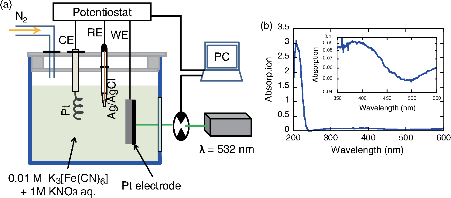 2.1.Preparation of the Pt Black ElectrodeA 30-nm-thick Ti film was deposited on the sapphire substrate to enhance the adhesion of the Pt film to the substrate. Figure 3(a) shows a scanning electron micrograph of an electrode on which Pt was sputtered, as shown in the dashed square. Figure 3(b) shows an atomic force microscopy (AFM) image of Fig. 3(a); the surface roughness was . Fig. 3(a) Scanning electron micrograph (SEM) and (b) atomic force micrograph (AFM) show the surface of the sputter-deposited Pt electrode. The surface of the Pt black coating is shown in SEM and AFM in (c) and (d), respectively. Cross-sectional profiles along the white dashed lines in (b) and (d) are shown in (e).  Pt black was deposited on the Pt electrode using an electrodeposition method.11,12 To deposit Pt black on the Pt film electrode, 1 g of hexachloroplatinic (IV) acid () was dissolved in 100 mL of deionized water with 0.1 mL of concentrated hydrochloric acid used as a plating solution. A three-electrode setup was used, in which the working electrode was a Pt film electrode, the reference electrode (RE) was a electrode and the counter electrode was a Pt coil 0.1 mm in diameter and 200 mm in length. After 5 min of electrodeposition at , a 4.2-μm-thick layer of Pt black was obtained on Pt electrode [Fig. 3(c)]. An AFM image [Fig. 3(d)] shows that the Pt black surface consisted of particles ranging from 30 to 70 nm and the surface roughness, , is 10.68 nm. A comparison of the cross-sectional profiles of the AFM images in Figs. 3(b) and 3(d) revealed a drastic increase in the surface roughness following Pt black deposition on the Pt film. 2.2.Current Generation EvaluationFigure 4(a) shows a cyclic voltammogram of the ferricyanide solution without laser irradiation, in which a constant current density was observed from to for the potential voltage with respect to that of the RE. To examine changes in current resulting from light irradiation, the photocurrent was measured at (versus RE) to exclude the effects of changes in conditions. Figure 4(b) shows the current density as a function of time. The laser irradiation was switched on and off every 100 s. As shown in Fig. 4(c), the average current density (circles) increased with laser power, , when the laser irradiation was on, whereas the average current density (squares) remained constant when the laser irradiation was off. Fig. 4(a) A cyclic voltammogram of ferricyanide solution is given without laser irradiation. (b) Current density is shown as a function of time. (c) Average current density is shown as a function of incident light power.  The blue circles in Fig. 5(a) show the normalized current density , where is the differential current density averaged between on and off states of the laser. To estimate the current generation without thermal heating, we calculated the heat generation in a Pt black electrode deposited on a sapphire substrate. Here, we consider the maximum temperature increase when the incident light was transformed completely into heat at the Pt interface by neglecting the solution without the reflection and transmission of light. In addition, the temperature at the interface between the back side of the sapphire substrate and the solution reached room temperature because the substrate was dipped in the solution. Based on these assumptions, one-dimensional conductive heat transfer model was generated using a simple structure [Fig. 5(b)] in which the heat transfers from the front (Pt film) to the back (sapphire substrate) of the electrode. The temperature rise , which is the temperature difference between the front and back sides of the electrode, is given1 where and are the respective thicknesses of the Pt () and sapphire () layers, and are the respective heat transfer coefficients of the Pt () and sapphire () layers, is the surface area of , and is the incident light power. As a result, we obtain .Fig. 5(a) Normalized current density is shown as a function of incident light power. The solid circles contain the error bars. (b) A diagram shows the calculational model of the electrode structure consisting of Pt (thickness ) and sapphire substrate (thickness ). (c) The difference between the obtained normalized current density [solid circles in (a)] and calculated current generation using [solid curve in (a)] is shown as a function of incident light power. The red solid line shows the fitted curve for .  The temperature dependence of the current density follows an Arrhenius-type behavior (, where is the current density, is the quasi exchange current density of the material, is the solvent rearrangement energy, is the gas constant, and is the temperature). The temperature-dependent rearrangement energy of the solvent can be determined by measuring the current with a constant applied voltage. Using a three-electrode setup, the current density was measured at (versus RE) over a temperature range of 278–328 K, and was found to be 0.39 eV. This value agrees well with the value of 0.48 eV calculated using the following equation: where is the diameter of a molecule (4.1 Å), is the refractive index of water (1.33), and is the relative permittivity of water (78.5). In addition, the temperature increase with light irradiation is considered to converge on a constant temperature of . Therefore, the increase in current can be described as follows:After using obtained above, the maximum current increase with laser heating is determined as follows: The solid curve in Fig. 5(a) shows the calculated current generated using . Figure 5(c) shows the difference between the obtained normalized current density [solid circles in Fig. 5(a)] and the calculated current generation using [solid curve in Fig. 5(a)]. The results indicate that heat generation was dominant at . Therefore, the difference between the calculated results and the experimental data may be due to the heat generation. To decrease this effect, we decreased the irradiation power. Figure 6 shows the normalized current density as a function of the incident light power. Here, we calculated the heat generated in a Pt black electrode using Eq. (4) (solid lines in Fig. 5) and found that the heat generation was negligible with respect to that of the phonon-assisted process. Differences in the Pt black electrode relative to that used to generate the data in Fig. 5 resulted in the off current density and consequent different values for . Note, however, that higher-order dependencies on the excitation power appeared with increasing current density, which were fitted by the second-order function (Fig. 6), indicating the two-step activation of electron transfer that originated from the DP on the nanostructured surface of the electrode. In addition, the current increase with the Pt black electrode was much larger than that on the sputtered Pt electrode [black solid curve in Fig. 6(a)], indicating that the current increase for Pt black originated from the DP on the Pt black surface. Fig. 6The relationship between irradiation power and current density is given at (a) and (b) . Solid squares correspond to the observed current generation for platinum black. Solid lines are the observed current generation for sputtered platinum. The solid squares include the error bars. The blue solid curves are line fits defined by (a) and (b) . The red dashed curves show the calculated heat generation using Eq. (4).  3.Concluding RemarksWe performed phonon-assisted activation of electron transfer using Pt black electrodes in ferricyanide solution under visible light irradiation. We evaluated the incident light power dependence of the generated current density and found it had second-order dependency, which indicated the two-step activation of electron transfer originating from the optical near-field effect on the nanostructured electrode surface. Since the phonon-assisted near-field effect can be enhanced when the structure is fabricated using the phonon-assisted near-field effect,8 further increase in photocurrent generation is expected using Pt black electrodes deposited using the phonon-assisted near-field process. Recently, Wada et al.13 achieved direct observation of DP generation with coherent phonons in homojunction-structured Si light-emitting diode in which modes of coherent phonons were determined using pump–probe spectroscopy. In addition, the side band originated from the coherent phonon excitation were observed in the spectra in Si LED, which was fabricated in a DP-assisted annealing process.14 By applying this technique to the electrode fabrication process, an optimum morphology can be achieved. This finding is not a quantitative innovation that enables improved electron transfer but is a qualitative discovery that opens new avenues in nanoscale physical chemistry. AcknowledgmentsK.I., K.K., and T.I. performed the measurements and K.I. analyzed the data together with T.K., and T.Y. prepared the manuscript. The authors thank Prof. Motoichi Ohtsu (University of Tokyo), for his active support and discussions. This work was partially supported by a Grant-in-Aid for Young Scientists (A) and Challenging Exploratory Research by the Japan Society for the Promotion of Science (JSPS). ReferencesP. W. AtkinsJ. de Paula, Physical Chemistry, Oxford University Press, Oxford
(2009). Google Scholar
R. A. Marcus,
“Electron transfer reactions in chemistry. Theory and experiment,”
Rev. Mod. Phys., 65
(3), 599
–610
(1993). http://dx.doi.org/10.1103/RevModPhys.65.599 RMPHAT 0034-6861 Google Scholar
M. Arenzet al.,
“The effect of the particle size on the kinetics of CO electrooxidation on high surface area Pt catalysts,”
J. Am. Chem. Soc., 127
(18), 6819
–6829
(2005). http://dx.doi.org/10.1021/ja043602h JACSAT 0002-7863 Google Scholar
R. M. Riouxet al.,
“High-surface-area catalyst design: synthesis, characterization, and reaction studies of platinum nanoparticles in mesoporous SBA-15 Silica,”
J. Phys. Chem. B, 109
(6), 2192
–2202
(2004). http://dx.doi.org/10.1021/jp048867x JPCBFK 1520-6106 Google Scholar
Y. Xuet al.,
“Adsorption and dissociation of on Pt–Co and Pt–Fe alloys,”
J. Am. Chem. Soc., 126
(14), 4717
–4725
(2004). http://dx.doi.org/10.1021/ja031701+ JACSAT 0002-7863 Google Scholar
K. Kobayashiet al.,
“Near-field optical potential for a neutral atom,”
Phys. Rev. A, 63
(1), 013806
(2000). http://dx.doi.org/10.1103/PhysRevA.63.013806 PLRAAN 1050-2947 Google Scholar
H. Fujiwaraet al.,
“Nonadiabatic multi-step excitation for the blue–green light emission from dye grains induced by the near-infrared optical near-field,”
Appl. Phys. B Lasers Opt., 98
(2–3), 283
–289
(2010). http://dx.doi.org/10.1007/s00340-009-3762-y APBOEM 0946-2171 Google Scholar
T. Kawazoeet al.,
“Highly efficient and broadband Si homojunction structured near-infrared light emitting diodes based on the phonon-assisted optical near-field process,”
Appl. Phys. B Lasers Opt., 104
(4), 747
–754
(2011). http://dx.doi.org/10.1007/s00340-011-4596-y APBOEM 0946-2171 Google Scholar
G. A. Tsirlinaet al.,
“Electroreduction of [Fe(CN)6]3 on a Mercury electrode: substantiating activationless character of the process at high overvoltages,”
Russ. J. Electrochem., 37
(1), 15
–25
(2001). http://dx.doi.org/10.1023/A:1009067309773 RJELE3 1023-1935 Google Scholar
M. H. ChakrabartiE. P. Roberts,
“Analysis of mixtures of ferrocyanide and ferricyanide using UV-visible spectroscopy for characterisation of a novel redox flow battery,”
J. Chem. Soc. Pak., 30
(6), 817
–823
(2008). JCSPDF 0253-5106 Google Scholar
B. Yazici,
“Hydrogen evolution at platinum (Pt) and at platinized platinum (Ptz) cathodes,”
Turk. J. Chem., 23
(3), 301
–308
(1999). TJCHE3 1300-0527 Google Scholar
L. Krishnanet al.,
“Platinum black polymer electrolyte membrane based electrodes revisited,”
J. Electrochem. Soc., 155
(9), B869
–B876
(2008). http://dx.doi.org/10.1149/1.2945231 JESOAN 0013-4651 Google Scholar
N. Wadaet al.,
“Measurement of multimode coherent phonons in nanometric spaces in a homojunction-structured silicon light emitting diode,”
Appl. Phys. A,
(2013). http://dx.doi.org/10.1007/s00339-013-7906-x APAMFC 0947-8396 Google Scholar
M. Yamaguchiet al.,
“Evaluating the coupling strength of electron–hole pairs and phonons in a 0.9 μm-wavelength silicon light emitting diode using dressed-photon–phonons,”
Appl. Phys. A,
(2013). http://dx.doi.org/10.1007/s00339-013-7904-z APAMFC 0947-8396 Google Scholar
Biography Takashi Yatsui received a BE degree from Keio University, Tokyo, Japan, in 1995, and ME and DE degrees from the Tokyo Institute of Technology, Tokyo, Japan, in 1997 and 2000, respectively. In 2008, he joined the University of Tokyo as an associate professor. He received the 2010 Gottfried Wagener Prize, the 2012 Osaka University Kondo Prize, and the 2012 Erlangen Innovation Award in Optical Technologies.  Kazaunori Iijima received a BE degree from the University of Tokyo, Tokyo, Japan, in 2010 and 2012, respectively.  Kokoro Kitamura received a DE degree from the University of Tokyo, Tokyo, Japan, in 2009. Since 2012, he has been an assistant professor at Shimane University.  Tadashi Kawazoe received a PhD in physics from the University of Tsukuba, Tsukuba, Japan, in 1996. He has studied optical nonlinearities in quantum dots at the Institute of Physics, University of Tsukuba. Since 2010, he has been a projected researcher at the department of electrical engineering and information systems in the graduate school of engineering at the University of Tokyo. |


