|
|
1.IntroductionNanowires (NWs) are quasi-one-dimensional (1-D) materials where one of the dimensions, usually in the 10- to 100-nm range, is much smaller than the other two (in the range of a few microns). They were first called nanowhiskers, but they have received other names in the literature such as nanorods or nanocolumns. They can be made of metals, polymers, or semiconductors, and the most common cross-sections are nearly cylindrical, hexagonal, triangular, or squared. The NW geometry has several advantages as compared to quantum wells or quantum dots, the most elemental one being the large surface-to-volume ratio as compared to a thin film (additional contribution of the lateral surface). Depending on the density and cross-section, an NW bunch can have 100 times more surface than a thin film of the same dimensions. This fact can be useful in the development of solar cells or chemical sensors.1 On the other hand, new concepts of heterostructures arise from the NW shape, like core/shell or axial heterostructures (quantum dots in a wire). Core/shell nanostructures can be particularly useful in the development of solar cells,2 while axial heterostructures are suitable for quantum computing.3 Semiconductor NWs can be grown by chemical vapor deposition, chemical beam epitaxy, or molecular beam epitaxy.4–6 Usually, they are grown using gold as a catalyst,7 but depending on the semiconductor, they can also be grown without a catalyst.5 They are commonly grown on a convenient substrate like Si or GaAs, which can be prepatterned in order to develop ordered NW arrays.1 Due to the existence of a free surface, heterostructures can be grown with larger lattice mismatch than superlattices or quantum wells.8 The reason is the relaxation of the structure at the sample surface.9 In very thin NWs, the fact that the bond distances close to the surface are larger due to relaxation effects produces changes in the electronic band structure of the material. NWs have a huge amount of applications—in photonic as light emitting diodes or lasers, solar cells, as energy harvesting materials,1,2 in transport as single-electron transistors,3,10 or in phototransport devices.11,12 One more particularity of semiconductor NWs is the fact that the balance between surface energy and bulk energy gives rise to new crystal structures, not stable when grown in bulk systems. In particular, most of the III–V semiconductors crystallizing in the zincblende (ZB) structure in bulk develop the wurtzite (WZ) structure when growing in the form of NWs;7 actually, very often, ZB staking faults appear within the WZ structure. A recent experiment on InAs NWs photoluminescence13 shows the existence of two bands in the emission at low temperatures, presumably one with origin in the ZB region and a second from the WZ region. From this variation, an energy gap of 2.45 eV for the gap of InAs has been obtained. This value is in very good agreement with resonant Raman measurements14 and ab initio calculations.15 High-resolution transmission electron microscopy images clearly show the existence of these two regions. The same behavior has been observed in other semiconductors, like InP.6 A detailed band structure calculation in the WZ phase has been performed in these two compounds.15,16 Figure 1 shows a set of InN NWs grown by molecular beam epitaxy under different temperatures, nitrogen flux, and In vapor pressure conditions. We can observe how the shape of the NWs can be completely different depending on the growth conditions. Fig. 1Indium nitride NW morphologies obtained under varied metal flux and substrate temperature (thermocouple temperature using the with opening) and constant growth time of 300 min and nitrogen flux ( at 0°C at 1 atm of pressure) and a plasma excitation power , which corresponds to a growth rate at stoichiometry of . Arrows indicate the modifications produced with the increase of the substrate temperature . (The author thanks Dr. Christian Denker for providing some SEM images of his PhD dissertation.)  Finally, the electronic bands bend at the surface of the NWs as in any surface in a solid, but in the case of an NW the effect is more notable due to the large contribution of the surface compared to the inner part of the NW. Although the origin is not completely clear, some NW semiconductors have a depletion layer at the surface, some others an accumulation layer.5,17 The accumulation layer influences both the optical18 and transport properties.19 In this first work, we will focus on the theoretical development of the Raman theory, first in bulk and then particularizing for the case of NWs. In a second work, we will pay more attention to the comparison of the existing theories with the available experimental results. 2.Raman ScatteringIn a semiconductor, most of the incident radiation is either reflected, absorbed, or transmitted; only a small amount is scattered. The elastically scattered light is called Rayleigh scattering. Actually, the elastic scattering is possible due to the existence of defects in the sample; in a nearly perfectly grown material with translational symmetry, the elastic scattering must be very low.20,21 A tiny amount of the scattered light, in general several orders of magnitude smaller than that scattered elastically, corresponds to inelastic light scattering or Raman scattering. The Raman effect or light scattering was predicted by Smekal in 1923 (Ref. 22) and measured simultaneously by Landsberg and Mandelstam,23 and by Raman and Krishnan24 in solids and liquids, respectively. Actually, the first set of authors discovered the effect previously, but the publication of the second set of authors appeared earlier in 1928. For this discovery, Raman was the Nobel laureate in physics in 1930. Raman was the only Third-World scientist who received the Nobel laureate for a research performed in an undeveloped country. Although the Raman effect is understood usually as the scattering of light due to phonons, any kind of inelastic light scattering is called Raman scattering. The scattering by electronic excitations or magnetic excitations are also Raman scattering. In this review, we are going to limit the analysis to the Raman scattering by phonons. The classical theory of the Raman effect was developed by the same authors who discovered the effect, Mandelstam et al.,25 and the quantum theory by Tamm.26 A rigorous development of the classical theory can be found in the book of Born and Huang.27 We will follow here the development of Cantarero et al.28,29 and Trallero-Giner et al.30 In the infrared, there is a direct coupling of the electric field of the light with the phonons, but in Raman scattering, the coupling is via virtual electronic states, as it was shown many years ago by Loudon.31 If the semiconductor gap is around the energy of the laser or scattered light, the transition between electronic states becomes real and the Raman signal increases orders of magnitude. In that case, we have to take into account the width of the electronic states, and the process is usually referred as resonant Raman scattering (RRS).28 Double and triple resonances (multiple resonances with several electronic levels) can also increase, additionally, the scattering signal.32 Electric fields,33 magnetic fields,34 or high pressure35 can also be tuned to produce RRS. Excitons play an important role in first-order RRS (Ref. 28) or Raman scattering by one phonon. In second-order RRS (scattering by two phonons at the -point), excitons also play a fundamental role in the resonant behavior36 because the intermediate excitonic state can also resonate. Electron–phonon interaction is thus the crucial part of the resonant process, since there is a direct interaction between the electrons and the phonons, even out of resonance. Electron–phonon interaction is actually very important within the electronic transitions itself since it renormalizes the electronic gap of the materials37 and gives a broadening to the electronic states. Also, when the electrons have enough energy to emit optical phonons, the photoluminescence processes become more efficient since the emission probability increases. Electron–phonon interaction is important not only in optics but also in transport, through the different relaxation mechanisms.38 The laser wavelength or laser energy is the other crucial part of the resonant process, since the variation of the laser energy approaching the electronic transition is the basis of the RRS. As an example, the Raman signal of strontium titanate/barium titanate (STO/BTO) quantum wells when illuminated with visible light was not good enough to even see the Raman signal. But ultraviolet light has been shown to be very efficient for analyzing STO/BTO quantum wells constituted even by a single layer39 due to resonance effects. In single wires, since there is a small amount of material, resonant effects are very important15 to make the Raman effect observable. In nonpolar semiconductors, there is no splitting between the the transverse (TO) and longitudinal (LO) optical phonons, but in polar semiconductors like GaAs, there is a splitting related to the difference between the low- and high-frequency dielectric permittivities (or the effective charges). The splitting is a measure of the polarity of the semiconductor. In polar semiconductors, plasmons interact with LO phonons giving rise to an anticrossing when the plasma frequency coincides with the LO phonon frequency, which depends on the electron concentration.40 From the measurement of the two split frequencies, the electron concentration can be obtained.40 In heavily doped samples, the electronic background is of the order of the Raman signal; electrons interact strongly with the phonons giving rise to the Fano lineshape,40,41 produced by the sum of quantum probabilities of the two processes, which can have opposite signs. Since phonons depend on the mass of the ions, Raman scattering has been used in the last years to study the isotopic composition of isotopically engineered samples42–44 and phonon anharmonicities.45 Phonons are also sensitive to pressure or stress variations.46,47 In thin films and semiconductor nanostructures, Raman scattering is used very often to obtain the lattice mismatch through the phonon deformation potentials.48 Recently, with the advances in the fabrication of holographic filters (notch or edge filters), a single spectrometer is enough to study the Raman scattering in most of the materials. A good holographic filter has a cutoff of , or even less. There are, in the market, several companies selling compact instruments, smaller than a shoebox, completely equipped connectable to a portable computer capable of obtaining reasonable Raman scattering signals at a competitive price. If we need to study phonon modes at lower frequencies, a double or triple spectrometer, in subtractive mode, is needed. Also, if we need to increase the resolution because the phonon lines are narrow, we can use a triple spectrometer in additive mode and lower the temperature to decrease the phonon anharmonicities. Most of the Raman systems are equipped with a charged coupled device, but if we really need resolution, we have to go back to the photomultipliers. In the book of Kuzmany,49 there is a complete description of the apparatus used in Raman scattering: spectrometers, gratings, and detectors. During the last decades, part of the scientific community has been dedicated to characterize, by Raman scattering, thin films, quantum wells, quantum dots, quantum wires, or even more complex nanostructures.50 In the simple case of a thin film, if we use the typical collection, a photographic camera objective, producing a laser spot , most of the Raman signal will come from the substrate and it can mask the really important signal. We need, in that case, the use of a microscope (micro-Raman or μ-Raman system), where the laser spot can be (with a confocal microscope, we can go to the diffraction limit50). However, the use of a microscope has a couple of disadvantages. First, all the light, including the reflected light, goes through the entrance slit of the spectrometer (unless we use a notch or edge filter). The second disadvantage is that the selection rules are not completely fulfilled. If we have an objective of and a numerical aperture50 , such as that shown in Fig. 2(a), the entrance angle with a refractive index of 3 (a typical value for semiconductors) will be . In a typical. μ-Raman system, a confocal microscope is employed in order to perform the measurements on a specific point of the sample (below 1 μm in lateral resolution and 100 nm in depth). A confocal microscope and a motorized xyz plate allow the mapping of small areas at different depths. In Fig. 2(b), there is a scheme of a confocal system where we observe how the light enters into a sample with a smaller angle due to the difference of refractive indices. Although we do not have a complete backscattering geometry, the selection rules are fulfilled to a great extent due to the difference in refractive index. Fig. 2(a) Cross-section of an objective (by courtesy of Carl Zeiss Microscopy, Germany). 1. Objective thread. 2. Stop face of the objective. 3. Spring system for the specimen-protection mechanism. 4. to 7. Lens groups for the correction of image errors. 8. Correction collar for adapting to deviating cover glass thicknesses or temperatures. 9. Front lens system. 10. Front lens holder. (b) Schematic representation of a confocal setup, where we can observe the angle change inside the sample due to the differences in refractive indices.  3.Scattering EfficiencyIn order to compare the Raman signal or the Raman intensity of different materials, it is convenient to use the Raman scattering efficiency (RSE), instead of the scattering cross-section, since the first amount is volume independent. In a polar binary compound semiconductor, the RSE per unit solid angle can be defined as28 where c is the speed of light in vacuum, μ the reduced mass of the ions, the volume of the unit cell, () the laser (scattering) angular frequency, () the refractive index at the laser (scattered) frequency, the angular frequency of the corresponding phonon, () the polarization vector of the laser (scattered) light, and the Raman tensor corresponding to the phonon mode. The factor has its origin in a quantum mechanical description of the phonon field,28 and it corresponds to the phonon emission (Stokes shift). In the case of phonon absorption (anti-Stokes shift or anti-Stokes scattering), the factor is . In practice, this factor is replaced by the Bose–Einstein distribution function, and this is the reason why at the anti-Stokes frequency, the Raman scattering signal is very weak as compared to that appearing at the Stokes shift, unless the temperature is very high. In a classical description, both Stokes and anti-Stokes components have the same intensity. An exception is stimulated Raman scattering, where phonons at the anti-Stokes frequency50 are excited. For Stokes shift, even if , the factor 1 remains and the Stokes shift can be observed at any temperature. The relative intensity of the Stokes/anti-Stokes Raman shift can be used to monitor the temperature.51The Raman tensor is a second-order tensor, sometimes written as a third-order tensor (or even as a fourth-order tensor52) contracted with the phonon polarization (, where is a unitary vector in the direction of the phonon displacement). The form of the Raman tensor depends on the symmetry of the crystal and the electron–phonon interaction, since in the Raman effect, electrons play a crucial role as virtual intermediate states in the Raman process.31 For an LO phonon propagating along ([1,0,0]) direction, the Raman tensor for the optical modes of a ZB crystal can be written in terms of the Raman polarizability as and it is observable in the scattering configuration written in Porto’s notation.53 Actually, we can write . The remaining nonzero Raman tensor components are . We will come back to this point in Sec. 4. The Raman polarizability has the expression54 where the relative phonon displacement is defined by the expression and is the amplitude probability of scattering of a phonon with wave number . The remaining quantities have been defined already. The amplitude probability where the of the Fermi golden rule has already been taken into account. This amplitude probability corresponds to the Feynmann diagram given in Fig. 3. The remaining five terms or Feynmann diagrams31 are nonresonant, and they can be neglected. () and () are the energy and broadening of the electronic states (which can be accessed in a time-resolved Raman experiment55). If there are several initial and/or final states (as it is the case of several valence bands in a ZB or WZ compound), we have to sum over after squares . The sum over intermediate states is performed before squaring the expression. and are the electron-radiation and electron(hole)-phonon Hamiltonians, which can be written in the second quantization formalism.28 The important point is the electron–phonon coupling constant, which consists of two parts, one corresponding to the emission of the phonon by the electron (see Feynmann diagram in Fig. 3) and a second corresponding to the emission of the phonon by the hole. In ZB- (and WZ-) type materials, only the second option is nonzero, and the electron–phonon coupling constant is where is the deformation potential (DP) matrix as defined by Bir and Pikus.56 In the case of the Fröhlich interaction,30 the basic expressions are the same; the only change is in the electron–phonon interaction Hamiltonian. Its coupling constant, in that case, is30 where the Fröhlich constant and (). Since Fröhlich is intraband (there is also an interband Fröhlich interaction with upper conduction bands—the electro-optic effect), we have to consider both contributions, that of the electron and that of the hole. We cannot do the dipole approximation () here, and the absolute value of must be taken into account. The Raman tensor for Fröhlich interaction is diagonal.It is interesting to realize that the DP is a local interaction, and thus it is related to the periodic part of the Bloch function, while the Fröhlich interaction, only possible in polar materials, is a long-range interaction related to the polarization charges in the medium, and only the envelope of the Bloch function contributes to the matrix element.30 On the other hand, since both processes are possible in the case of LO phonons, the amplitude probability must be added before squaring it, and interference effects can appear29 when the Raman polarizabilities corresponding to deformation potential (DP) and Fröhlich interaction are of the same order of magnitude, i.e., close to an electronic transition, in resonance. This is the reason we usually say that the selection rules are not completely fulfilled in resonance. During many years, the huge enhancement of Raman scattering close to the gap could not be explained, and it was attributed to unknown values of one of the constants that appear in the expression of RSE or to the existence of impurity-induced Raman scattering.57 Finally, it was demonstrated that the consideration of excitons, instead of electrons,31 as intermediate states in the Raman process could explain the absolute value of Raman scattering in the case of deformation potential,28 Fröhlich interaction,30 and also the interference between both.29 The interference is produced due to the fact that we have to add the probabilities before squaring (they correspond to different intermediate steps). 4.Raman Tensor and Raman Selection RulesIn Sec. 3, the Raman tensor of an LO phonon propagating along the [100] direction of the ZB structure was defined in Eq. (2). We also defined the remaining components of the Raman tensor using the conventional unitary vectors along , , and . If one is interested in a different crystal surface, a general method to proceed is to define the following three vectors:58 defining the crystal surface where the Miller indices are normalized (). The two perpendicular vectors forming a right-handed coordinate system areIt is also convenient to define the matrix formed by these three vectors written in rows. Following Fig. 4, the axis will be always along the direction, i.e., the incoming wave vector of the light and outgoing are along . The phonon wave vector , in backscattering configuration, will also be directed along . Thus, the LO phonon will vibrate in the direction, while the two TO phonons will vibrate along the and directions. The three vectors are unitary. As commented in Sec. 3, the Raman intensity will be proportional to Fig. 4Fix axes system, where we have chosen as the direction of the cylinder axis, as the direction of the light in backscattering configuration, and as the perpendicular direction, forming a right-handed system. The vectors and indicate the polarization of the incoming and scattered light, respectively, and and the corresponding angles of rotation, with origin in the axis with counterclockwise rotation. 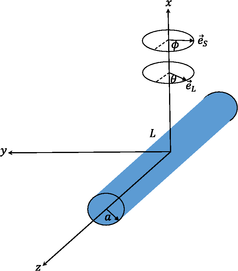 In the case of an LO phonon, the Raman intensity will be proportional to while in the case of TO phonons, the intensity will be proportional toThe reason of summing after squaring is that these are two different final states, but since they appear at the same energy when looking at the Stokes shift, we have to add the intensities. Of course, depending on the selection rules for a given surface, only one of them can contribute. In the case of the ZB structure, it is very simple to calculate the resulting intensity for a surface, for instance. In that case, If the polarization vectors and are both along the (110) direction, the transformed vectors are along the direction. The transformed Raman matrix .The Raman matrices multiplied by the phonon polarization, , in units of the Raman polarizability. The final result is , , . It is simple to check that, for , the result is , , and (the total contribution of the TO is ). The LO mode is forbidden for this configuration. These results are identical as that given by Cardona.52Although we have given a general procedure, we will pay particular attention to the case where one of the axis is along the [111] direction, the NW growth direction or the cylinder axis. The reason is that this is the equivalent to the [0001] direction of the WZ structure and the results can somehow be compared. Figure 4 shows the coordinate system where the NW axis is along the laboratory direction. In that case, it is better to select as for and surfaces, respectively. For a surface, if , , , i.e., the contribution of the TO mode is , while the LO mode does not contribute. If , the contribution of . As is well known, the LO phonon is forbidden in the case of a surface in a ZB material. If , and . In the case where , . For crossed polarizations, .Polar plots can be drawn by considering, in the case of surfaces, in agreement with Fig. 4, In the WZ structure, there are nine optical modes, but two of them are silent modes. The seven Raman active optical modes are drawn in Fig. 5. The first mode vibrates along the direction of the WZ structure. The Raman tensor is Fig. 5Raman allowed phonon modes in wurtzite-type crystals. The mode is 1-D while the E modes are 2-D 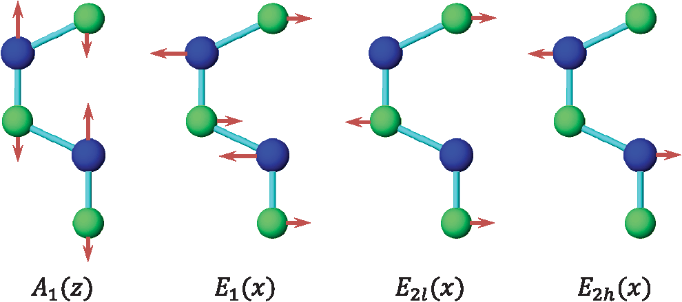 The 1-D mode is a polar mode, with a different polarizability when propagating in the direction or in the plane. As stated before, group theory gives only the difference in anisotropy ( and polarizabilities), but does not consider the splitting, which is due to the polarity of the medium. The two-dimensional (2-D) modes are also polar modes, with Raman tensor When propagating along , will be LO, while it will be TO if it propagates along . There are actually two bidimensional modes, but one of them corresponds to two acoustic modes, the third acoustical mode being a 1-D mode. There are also two nonpolar bidimensional modes, as can be observed in Fig. 5. Both modes actually mix, but the amplitude of the heavier (lighter) atom dominates in the () modes, vibrating at lower (higher) frequency. The corresponding Raman tensor can be written as The WZ is an anisotropic structure. At this point, it is interesting to remark that there are two kinds of anisotropic structures. In the first one, the crystal anisotropy dominates;59,60 actually is very different from . This is the case of most of the layered compounds,46 or nonpolar compounds like graphite, but the most common case is that where the Coulomb interaction dominates.35 This is the case of III–V compounds grown in the WZ structure. In recent cases where typical ZB crystals grow in the WZ structure, the material anisotropy is unkonwn, but, on one side, we know the splitting, i.e., the intensity of the Coulomb interaction, and on the other side, a small difference is expected in the crystal anisotropy since the structures are identical until second neighbors. This is very important when we want to draw polar plots in the case of WZ materials. When we rotate the polarization, the polar modes are mixed. Instead in a strongly anisotropic material, and [or and ] mix. Since we are interested in crystals with a small anisotropy, the Raman polarizabilities and will be taken as equal to simplify the final expressions, i.e., With this approximation, we can easily obtain the Raman selection rules in backscattering from the lateral side of a single WZ-NW grown along the c-axis. Looking at the picture given by Sander et al.,61 the axis is perpendicular to the -plane [ plane in three-index notation], while the axis corresponds to the -plane [(110) in three-index notation]. The axis is along , the [0001] direction ([111] direction of the ZB). The selection rules for a few standard configurations are summarized in Table 1. If one is interested in polar plots, we have to calculate the components of the Raman tensor. Let us do, as an example, the scattering configuration where is in the zy plane. The vectors and . Table 1Selection rules for backscattering configuration from the a plane (nanowire lying in a surface) and c plane (nanowire perpendicular to the surface or a bunch of nanowires).
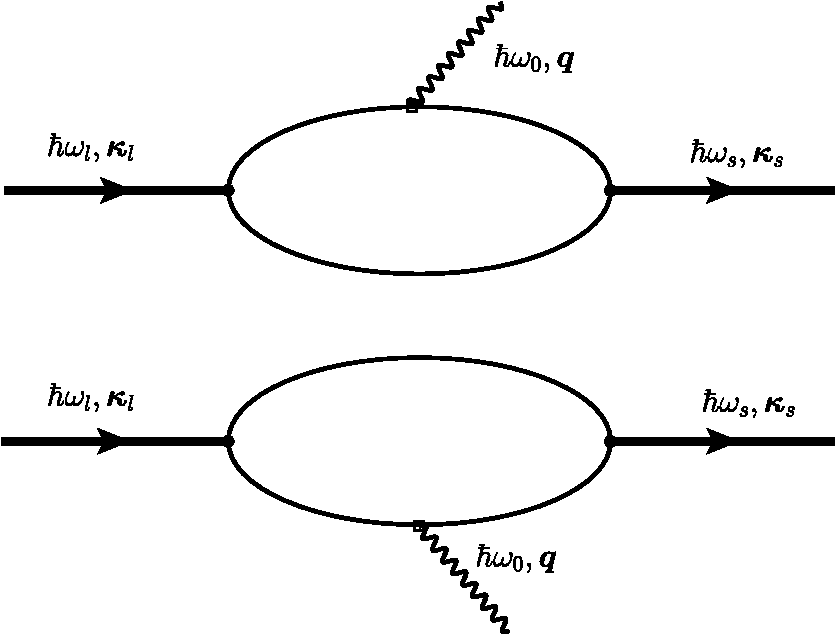
The Raman intensities will be, in the configuration, We have summed the squares (without considering any interference) since they are different phonon modes or different final states. However, we have to remember that they mix, and give an intermediate frequency between the and or the and the , in agreement with Eq. (25).5.Theory of Polariton Modes in a CrystalThe number of phonon modes in a crystal depends on the number of atoms in the unit cell. As is well known from a general course of solid-state physics, if a unit cell (primitive cell) has atoms, there are optical modes. Depending on the complexity of the crystal, we can have from a few to tens of optical modes. For instance, in silicon, there are three optical modes, as in ZB-type materials; in WZ materials, there are nine optical modes (seven are Raman active), while in a more complex material, like and isostructural layered materials, there are 57 optical phonons, 27 of them Raman active.62 In the case of an NW, there is no translational symmetry in the plane perpendicular to the NW axis. If the NW is very thin (a few nanometers of radius), we have confined modes (see Sec. 7). With increasing NW radius increases, the confined phonon modes overlap due to the finite linewidth, giving rise to an asymmetry at the low frequency region of the LO or TO phonon peaks. NWs of the order of several tens of nanometers can be considered, for most of the purposes, as a bulk material. Just as an example, in transport phonons can be treated as bulk materials even for NW diameters down to 30 to 40 nm.63 The only difference will come from the existence of a surface or an interface (core/shell NWs), giving rise to new phonon modes, the so-called surface optical (SO) modes. Let us start our discussion analyzing bulk phonons (i.e., there is no surface) in a solid. From group theory (at ), there is no splitting of the optical modes; LO and TO modes have the same energy. Actually, the splitting is produced at finite in polar semiconductors due to the coupling of the phonon field with the electromagnetic field of the light (phonon–polariton). In bulk materials, the polariton branches are derived from the solution of the Maxwell equations inside the material and the coupling of electric field produced by the phonon displacement with the electric field of the electromagnetic wave.64 From the LO to the TO frequencies, there is a forbidden region where the electromagnetic wave cannot propagate in bulk materials (the electromagnetic field is totally reflected). Actually, because of the losses (imaginary part of the dielectric function), the reflectivity is not exactly one in this region. Although the coupling between the ionic displacement in a polar crystal and the electric field of the electromagnetic wave of the light is produced directly in the infrared region of the spectrum, it can be analyzed by Brillouin scattering,65 and this coupling is responsible for the existence of surface modes, as we will see later. In a Raman experiment in backscattering geometry, , where and are the refractive index and wavelength of the laser light, respectively. For the typical green line of an Ar laser (), . In a Brillouin scattering experiment, the complete measurement range is below this amount. If we consider the harmonic movement corresponding to a phonon traveling along the crystal, the equation of motion will be that corresponding to the harmonic oscillator. On the other hand, if there is an electromagnetic wave in the polar crystal, there is a polarization vector proportional to the electric field, the proportionality constant being the electric susceptibility at a microscopic scale. But these fields are coupled through the ionic movement. Let be the vector displacement between the positive and negative ion in a simple polar semiconductor (as the ZB, for instance) and , ( is basically the density , the mass density). The equations to be solved in order to obtain both the electric polarization and the vector displacement due to the existence of the external field are Equation (28) must fulfill at the same time the Maxwell equations, which we write in the Gaussian system, for simplicity, and assume a plane wave solution , Combining these equations, we arrive to the solution At very high frequencies, the ionic movement cannot follow the electric field, only the electrons, and we arrive to the trivial solution On the other hand, uncoupled transverse phonons do not carry electric field and thus vibrate at their resonant frequency , thus . Finally, in static conditions (), we obtain from the coupled Eq. (28) The final expressions coupling the fields and atomic movement are Taking the displacement from Eq. (33), substituting in Eq. (34), and using Eq. (30) in the particular case of transverse modes (), we arrive at the following equation: Using Eq. (35), we arrive at the solution The solution of Eq. (36) is given in Fig. 6 using the data of GaAs.42 At , there are two solutions obtained from the last equation taking the limit : and . For large values of , we obtain, taking the limit , and . The longitudinal solutions are obtained assuming . From the coupled equations, . In Sec. 6.1, we will see how these equations are modified due to the existence of a limiting surface in the solid. The value of the electric field can be recovered from Eq. (28). In the case of TO modes, Eq. (28) gives , and for LO modes, We can follow the same strategy to analyze the polariton dispersion in a crystal with the WZ structure. There are two modes, which are Raman and infrared active, (a 1-D mode vibrating along the axis of the WZ structure) and (a 2-D mode vibrating in the plane perpendicular to the axis). In a uniaxial crystal, the dielectric function is a tensor, isotropic in the plane perpendicular to . Let us write We will restrict ourselves to the case where the phonons propagate along the axis and the axis ( is along or —the direction is equivalent to ). If , we have a mode and two degenerate modes (vibration along and ). If the phonons propagate along the (or ) direction, we will have the mode vibrating along and propagating along and two modes, a mode vibrating along and propagating along , the , and a second mode vibrating along and propagating along , the . Obviously, these two modes are not degenerate in that case. For the case where , the electric field can be along the axis (or ). In that case, Eq. (30) becomes The equations coupling the fields with the atomic movement are The same solution is obtained if the fields and ions vibrate in the plane [exchanging by in Eqs. (39) and (40)]. The solutions are the dispersion of the two degenerate modes. By solving the three equations, we arrive at a solution equivalent to that of Eq. (36), replacing by and by . The solution can be better written in an equivalent way as Eq. (30). The limits and are easily extracted from these equations, and , respectively (see Fig. 7). Here the electric field and the movement is along ; the solution is (), corresponding to the with frequency . These solutions are plotted in Fig. 7 for ZnO. If is along the axis, the mode propagating along the direction will be longitudinal, with frequency . The dispersion of the modes propagating along and are obtained by solving the equations respectively. The dispersion is shown in Fig. 7.In the figures with the polariton branches, has been written in wave numbers. In the case of Raman scattering, the value of is far away from the polariton region. In backscattering configuration and assuming that the selection rules are fulfilled (that depends on the cylinder radius), . For , the laser frequency in is . The scattered frequency, for instance, for Si is (515.909 nm). The value of will be (in the polariton region, ). 6.Surface Optical Modes6.1.Surface Optical Modes Within the Polariton DescriptionIn finite-size samples, there are additional conditions on the electric and the magnetic fields since they must fulfill the boundary conditions at the sample surface. The existence of these boundary conditions generates additional solutions in the polariton equations. In general, there is a complete set of solutions ranging from below the TO to above the LO region, depending on the geometry. Let us consider a single cylindrical semiconductor NW of radius , with a dielectric permittivity , and an electromagnetic field with time dependence . If the external medium has a dielectric permittivity (in case of air or vacuum, ), the electric and magnetic fields outside and inside of the NW must fulfill the Helmholtz equations. inside the material and outside the material. The Helmholtz equation can be solved exactly in six coordinate systems,67 in particular, in cylindrical coordinates. In case of a hexagonal cross-section, the main conclusions from this section will not vary, but the calculation of the electromagnetic field must be done numerically due to the complexity of the boundary conditions.Let us call and . Equations (44), in cylindrical coordinates, become, for a scalar function , inside the material. Outside, we have to replace by . By assuming a solution of the type , we arrive at the equation where [or outside the crystal] and whose solutions are Bessel functions of first class [], second class [], also called Neumann functions, and third class [ or ], or Hankel functions. Inside the cylinder, the solution is of the type (analytical at the origin), and outside the cylinder, it is more convenient to take Hankel functions [], i.e., where we have removed the superindex of the Hankel function for clarity. The Hankel functions can be expanded in plane waves.68 We are interested in the absorption (transmission, scattering) of a plane wave (laser beam) by a semiconducting cylinder.It is also possible to assume a conducting hollow of radius , . In that case, the solution outside the cylinder will be Neumann functions. Once we have the solution for the Helmholtz scalar equation, those for the vector equations are easily obtainable. For instance, following Ref. 68, two vector solutions are where is the solution of the scalar equation. The modes cannot, in general, be split into transversal electric and magnetic; they are mixed through the boundary conditions (due to the existence of a surface). In the general case, the eigenfrequencies are obtained by solving the equation60However, the most interesting case corresponds to the analysis of a single NW when the light incides in the plane. In that case, and the scalar function does not depend on . Let us suppose that the electromagnetic wave has the electric field component along . Since the tangential component of must be conserved, . From the Faraday equation, . Since we are considering a nonmagnetic medium, both the normal and tangential components of will be continuous when crossing the surface. We arrive at the following three equations corresponding to the continuity of , , and : where the first two equations are the same. By solving the equation for the coefficients and ,The modes solution of this equation are called -polarized. On the other hand, if the magnetic field has only a component, we have to use the fourth Maxwell equation , where the displacement vector inside the material and outside. From the continuity of the tangential component of , the normal component of , and the tangential of , we arrive at the equations The transcendental equation for the -polarized modes is These equations give a set of eigenvalues below the TO frequency, in the gap between the TO and the LO, and above the LO. In the limit , the solutions are very simple. In the case of -polarized modes, for , there is only one solution, , the bulk solution. When increases, a number of solutions appear below the TO region. For increasing , there are solutions in the gap and above the LO region. But for thin NWs, there is only one solution, . In the case of -polarized modes, there are no crossing points for . In other words, for , there is only one solution, which corresponds to the bulk mode in the -polarized case. For , and , the solution of Eq. (56) gives corresponding to . Actually, in the range between and , where the dielectric function is negative, the Bessel function ; it can be written in terms of the modified Bessel function. In Fig. 8, we have plot the dielectric permittivity for GaP [ and , and (Ref. 69)] as a function of . As must be expected, the dielectric function diverges at and becomes negative for until , where it becomes zero. Two dashed lines indicate the limits and (calculated from the Lyddane–Sachs–Teller relations with the data supplied in Ref. 69). In the inset, we show the region close to , where we can observe the surface optical modes. The horizontal lines correspond to and , obtained from the transcendental Eq. (56) taking . The vertical lines are the different frequencies, which can be calculated accurately with Eq. (56). We can observe how the frequency of the surface mode shifts down depending on the external or surrounding medium. From air to a surrounding medium with , there is a shift of .Fig. 8Real part of the dielectric permittivity, as a function of in the region of interest between the TO and LO. At the TO frequency, there is a divergence, and at , the dielectric function is zero. Three optical surface frequencies corresponding to external media with (air), , and with the data of GaP.69 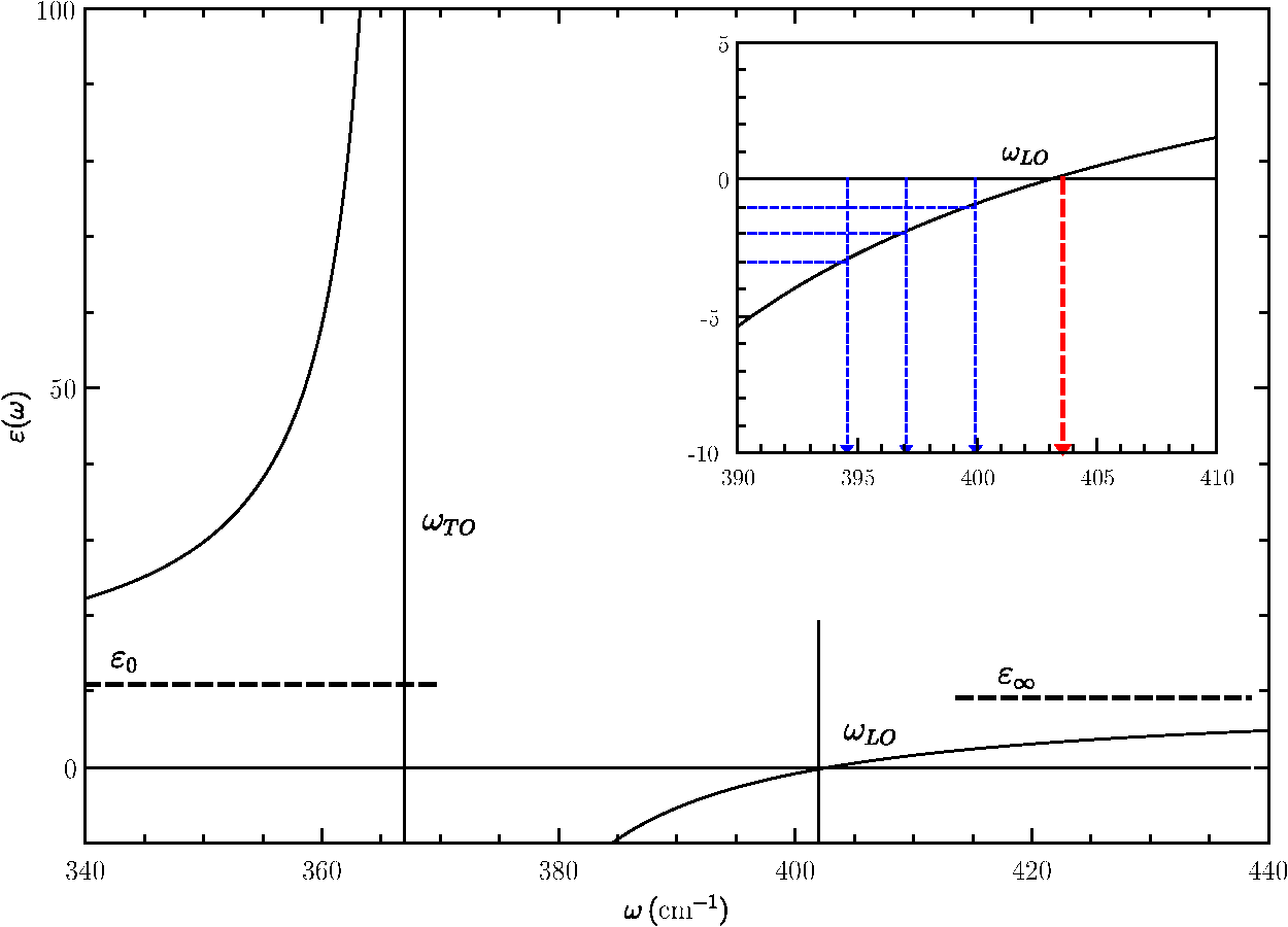 We will compare this result with that given in Sec. 6.2, neglecting retardation. We have to keep in mind that the first surface optical mode is obtained when the electric field is perpendicular to the NW direction, and it corresponds to the solution of Eq. (56). In the case , there is no crossing point. In the case of -polarized modes (), we obtain the bulk solution () in small diameter NWs. 6.2.Surface Modes Within the Nonretarded LimitThe advantage of writing the Maxwell equations in the Gaussian system is that the nonretarded limit is obtained simply with the limit . In other words, the magnetic field contribution is neglected. Since , we can write . On the other hand, we have . Inside the material, , while outside the material . In both cases, we can write , and we arrive at the Laplace equation instead of the Helmholtz equation for the surface modes.60 where is the electrostatic potential. Actually, we are also assuming that , i.e., there are no volume polarization charges. In cylindrical coordinates, this equation can be solved by separation of variables, considering where is the axis of the cylinder and the phonon wave vector along the z direction. Substituting into Eq. (58) and multiplying by , by choosing . Rewriting the equation in terms of , whose solutions are the modified Bessel functions and . Since when and when , the potential has the solution where and are constants indicating the strengths of the fields. Once we know the potential, we can calculate the electric field, which in cylindrical coordinates isAt the surface of the cylinder (), the boundary conditions for the fields (, , and ) must be fulfilled. This requirement gives rise to the following two equations: The last two equations are identical. Solving the first two equations for and , Appealing to the expression for the dielectric function and using Eq. (65), the following useful expression can be derived: where correspond to the different surface modes. This expression has been written in the literature in several ways, most commonly in terms of the plasma frequency. It should be pointed out that one of the most common references on surface modes has an error; in Eq. (7.41) of Sernelius’s book,70 the case may correspond to and not to 0 since the dielectric function diverges at . On the other hand, since we have also found a mistake in a commonly used mathematical table,71 we write down here the expressions of the derivatives of and , which are actually different.The correct expressions can be checked, for instance, in the book of Arfken et al.67 Taking the limit , we obtain the expression found in many text books.72 Actually, if (there is no propagation in the direction), we have the same result, which was previously found in the retarded limit. The solution corresponding to is the bulk solution (, corresponding to ), while that corresponding to is the -polarized mode.60,73 In Fig. 9, we can see in the left panel (a) the three first solutions of Eq. (67). For a fixed , as soon as increases, we move from the bulk solution () of the cylinder to the solution of the slab (when the radius of the cylinder ), and there is no difference between and parallel to the other in plane coordinate. For small radius (), the first surface mode corresponds to and it is -polarized; the electric field component will be along . In Fig. 9, right panel, we have drawn the first surface phonon solution, for , a material surrounded by air. Assuming, as an example, and (see end of Sec. 6), a NW of , and a numerical aperture of , following the deduction at the end of the Introduction, to 0.03. Looking at Fig. 9 (right panel), the SO mode will be nearly at the same value as that calculated by the usual expression. Actually, this calculation corresponds to the maximum value of ; thus the SO mode must be in between the value corresponding to and the maximum . In summary, we can neglect any deviation from Eq. (57). Obviously, is conserved in an infinite cylinder and the Raman selection rules must be fulfilled.Fig. 9(a) The solid line corresponds to the mode, converging to at (). (b) Detail of the dispersion of the first SO mode () using the experimental data of InAs.15 The calculation of is explained in the text. The corresponding energy for to 0.03 gives a small energy shift toward lower energy, although negligible.  7.Raman Scattering by Confined Optical ModesThe dielectric continuum approximation and the dispersive hydrodynamic model have been used in the past to describe the optical confined modes in several kinds of heterostructures.74,75 They predict different symmetry patterns for the electrostatic potential and the phonon displacement. In an isotropic continuum model, the LO and TO phonons are decoupled in bulk materials, while, as we have seen in Sec. 6, they couple in the general case due to the existence of a surface that mixes them, and new modes related to the surface (surface optic modes) appear. The existence of SO modes can also be related to the cut-off in the Coulomb sum since the crystal is not infinite. We have already written the basic equations needed for the study of the confined modes in a cylindrical quantum wire; they are given by Eqs. (33) and (34). The behavior of these modes (if decoupled) moving along the cylinder axis is basically that of bulk modes due to the existence of translational symmetry. The phonons produce a deformation, which can be accounted for by including the stress tensor in the basic polariton equations. In Sec. 6 we have neglected this contribution. Actually, we have to modify Eq. (33) slightly to include the existence of local strain. In Ref. 74, we started with the Lagrangian formalism, but, basically, we have to modify Eq. (33) to the final form. where we have assumed an dependence and introduced , the mass density, in order to keep the definition of the mechanical stress tensor .Equation (34) can be rewritten as Using the first Maxwell equation,The physical boundary conditions at the interface of the cylinder with the external medium (with dielectric constant ) must be
On the other hand, we consider the dispersion of the LO and TO modes in the plane in the simple way and , where the LO and TO modes are related through the Lyddane–Sachs–Teller relations, . The parameters and indicate the curvature of the phonon branches, and the wavenumber has been labeled or to distinguish between the phonon branches. We will see later that they are related to the sound velocity. In order to simplify the description, we assume an isotropic elastic medium, with two elastic constants (Lamé coefficients and ). In terms of the conventional elastic compliances, On the other hand, the transverse and longitudinal sound velocities in a solid are In terms of the sound velocities, Introducing the Lamé coefficients into the stress tensor and replacing the sound velocities and by the coefficients and , Eq. (70) can be written as where we have made use of the identity . The solution of this complicated equation was solved by assuming74 where the additional condition was imposed.75 After a little algebra, we arrive at the following set of four coupled partial derivative equations in cylindrical coordinates:Assuming [we are interested in the confined modes within the NWs (there is no confinement along )], , and we can assume [and ]. The displacement can be written as The four coupled systems of equations reduce to two coupled equations, with solutions where both functions and are solutions of the Laplace equation. The phonon displacements and the electrostatic potential are coupled through the two solutions.The general solution of these equations have been already given in Ref. 75; here, we give only the secular equation. where the arguments are The variable is given by and the functions andBy solving these equations, we are able to find the complete set of eigenvalues for the different values of . The eigenvectors are obtained by introducing the corresponding eigenvalues into the expressions of the displacement and electrostatic potential.75 In previous works,74,75 we have analyzed the case of an FSW, surrounded by air, and what we called a quantum wire, embedded in a different semiconductor, in that particular case, GaAlAs. In that case, there are two surface and two boundary conditions. In the interface between the two semiconductors, the boundary conditions are the same as that previously discussed; in particular, the normal component of the stress tensor is continuous at the interface. In the external surface, the normal component of the stress is zero. There are two kinds of modes: interface modes located at the interface between the two semiconductors and a surface mode located at the external surface of the NW. Li has analyzed this last case of a core/shell NW for a GaAs/AlGaAs NW.76 The difficulty arises because in the region of the shell, both the Bessel and Neumann functions are valid and the boundary conditions become a little bit cumbersome. In the work of Li,76 he uses the first and second kind Bessel functions. In this last paper, Li limits the study to the interface and surface mode. Figure 10 shows the confined phonon modes as a function of the cylinder radius. In the upper panel, the case where a GaAs NW is embedded in AlGaAs is shown for the case , , and . For , for instance, for , there are only two confined modes in the region between the LO and TO, but as soon as the radius increases, the number of modes increases rapidly. For , there are already 16 modes in that region. We observe two sets of curves, one converging to the bulk and a second one converging to the bulk value of LO phonons . Starting in , as we have commented in Sec. 6.2, the confine modes mix with the surface modes. In Ref. 74, this anticrossing can be observed more clearly since there are a few modes drawn and the decoupled modes have also been drawn. The calculation, for the GaAs/AlGaAs NW, corresponds to the expression and being GaAs and AlGaAs (or vacuum in the case of an FSW). We called the frequency of the surface or interface mode because Fröhlich77 did the calculation for the first time for the case of a dielectric sphere embedded in a second dielectric. The values obtained were in the GaAs/AlGaAs NW and for a GaAs NW. It is interesting to realize, also, that in the case of , the surface modes do not appear, as commented in Sec. 6.2. The reason is that, for , the transcendent Eq. (82) decouples into two equations and the LO and TO phonons do not mix as in the case of an infinite material. For , there is a strong mixing of the LO and TO phonons, as can be observed, for instance, in the mode just below the bulk TO phonon limit in the case of the FSW. For , we clearly observe the surface optic phonon, which consists of a homogeneous polarization of the NW []. At this frequency [that given by Eq. (87)], there is no difference between longitudinal or transverse modes. Figure 11 shows the dispersion of a GaAs NW surrounded by AlGaAs when . We clearly see the surface mode, which appears at an intermediate frequency due to the large value of the external dielectric constant (constant in the region of GaAs phonons). We have also plotted the uncoupled solutions corresponding to bulk. We can see the surface mode, interface mode in that case, as a new solution due to the mixing of the LO and TO solutions, due to the existence of a surface or an interface.Fig. 11Dispersion in a GaAs nanowire embedded into AlGaAs (Ref. 74) in the case . We have drawn the decoupled solutions, as explained in the text.  In Ref. 75, the Fröhlich electron–phonon interaction Hamiltonian has been deduced for the case of confined phonons, both for free-standing NWs and NWs embedded in a different material (interface modes). Li76 has calculated the interface and surface modes for a core/shell NW neglecting confinement effects. He has also obtained the Fröhlich electron–phonon Hamiltonian. Since the number of confined modes increases drastically as soon as the NW radius increases, we basically have a continuity of modes since they cannot be spectroscopically separated. At 6 or 7 nm, we already have a continuity of modes, which can be observed in Raman as a broadened line. An example is the measurement reported by Zhang et al.78 in Ge NWs. They group the NWs into a range of sizes and the Raman spectra are asymmetric, indicating either confinement or a smaller signal coming from the smaller NWs. In their Fig. 5, they show the Raman spectra of a set of NWs with diameters from 6 to 17 nm. Clearly, even with these diameters, wave vector is conserved, otherwise the one-phonon density of states would be visible. A theoretical study on nanoparticles, and also on 2-D and 1-D systems, was performed by Faraci et al.79 The theoretical results show how a nanoparticle with a diameter of 10 nm has basically the same Raman spectrum as a 7-nm nanoparticle. In the case of 1.5- or 2-nm nanoparticles, the shape is asymmetric as commented in the case of Ge NWs. The width is compared for the case of three-dimensional (nanoparticles), 2-D, and 1D, which shows a smaller influence in the case of NWs (smaller shift) than in the case of nanoparticles. 8.Antenna EffectIn bulk materials, the light penetrates into the semiconductor depending on the absorption coefficient (or imaginary part of the dielectric function). The penetration depth in GaAs, close to the critical point, is . In general, even if the NW diameter is , a direct gap semiconductor strongly absorbs the light above the band gap (i.e., in resonant conditions). However, the Raman intensity does not follow the classical selection rules in very thin NWs. There is a typical dipole dependence, and the maximum Raman signal is obtained when the polarization of the laser light is parallel to the NW axis. This behavior was observed for the first time in 2000 in single-wall carbon nanotubes,80 and it was already predicted by Ajiki and Ando in 1994.81 Although there are several observations of this phenomenon, denominated antenna effect, in the literature in several semiconducting NWs, a couple of interesting works should be mentioned. The first one is a review of Xiong et al.,80 where they summarize a set of experimental works done on GaP NWs ranging from 50 to 200 nm in diameter. They observe that the strong polarization disappears when the diameter of the nanowire is nm for the laser line used in the experiment (488 nm). The diameter is too large to be related to electron confinement effects. For NWs of 105 nm in diameter, they observe a behavior, while in a 160-nm wide NW, the emission has a multipolar character. In order to explain the observed behavior, they used the discrete-dipole approximation80 to calculate the light absorption. In this approximation, the NW volume is replaced by a set of dipoles, which vibrate or interact with the incident electric field. In Fig. 12, we reproduce the electric field maps of two NWs 200 and 500 nm in diameter. In the NW with (left panel), the electric field penetrates into the nanowire in both cases, when (up) and in a small amount when (down). In the case of a NW, the electric field basically is zero inside the NW (panel right, down). Fig. 12Electric field intensity maps around the cross-section of GaP nanowires calculated using the discrete dipole approximation.82 The two upper panels correspond to E-polarization (electric field along the wire), while the lower panels correspond to H-polarization (electric field perpendicular to the wire axis). The wire diameter of the two panels at the left is 200 nm, while that at the right is 50 nm.  There is a second interesting paper,83 where they calculate the polarized-Rayleigh backscattering signal instead of the complicated Raman signal, where we have to additionally take into account the Raman selection rules. Although unfortunately there are no explicit calculations (they refer to the original work of Rayleigh in 1881), they show that there are different resonances as a function of the NW diameter and also show the polar plots for a set of NWs, ranging from to 560 nm. The results are in close agreement with the experimental results of the experiment performed by Xiong et al.82 Nevertheless, a complete quantum theoretical approach is still needed. 9.ConclusionsIn this review paper, we have described the main topics related to Raman scattering in semiconductor NWs. After a revision of Raman scattering efficiency, we have found the selection rules, in particular, for the two interesting cases of ZB and WZ materials. We have summarized the theory of surface optical phonons, comparing the results including retardation effects and the simple expression found in the literature where retardation is neglected. This expression has been used incorrectly and many unphysical results have been obtained. We also studied the case of phonon confinement and the appearance of the SO modes starting in the phonon; since in the case of we have shown that even in the presence of a surface, LO and TO modes do not mix. Finally, we give a short description of the antenna effect, although more effort must be put in this direction in order to give explicit analytical expressions. AcknowledgmentsThis work has been soported by Grants MAT2012-33483 and CSD2010-0044 of the Programme Consolider Ingenio of the Ministry of Finances and Competitiveness of Spain. ReferencesC. M. Lieber,
“Semiconductor nanowires: a platform for nanoscience and nanotechnology,”
MRS Bulletin, 36 1052
–1063
(2011). http://dx.doi.org/10.1557/mrs.2011.269 MRSBEA 0883-7694 Google Scholar
P. YangR. YanM. Fardy,
“Semiconductor nanowire: what’s next?,”
Nano Lett., 10 1529
–1536
(2010). http://dx.doi.org/10.1021/nl100665r NALEFD 1530-6984 Google Scholar
V. S. Pribiaget al.,
“Electrical control of single hole spins in nanowire quantum dots,”
Nat. Nanotechnol., 8 170
–174
(2013). http://dx.doi.org/10.1038/nnano.2013.5 1748-3387 Google Scholar
Y. J. Hwanget al.,
“ core/shell hierarchical nanowire arrays and their photoelectrochemical properties,”
Nano Lett., 12 1678
–1682
(2012). http://dx.doi.org/10.1021/nl3001138 NALEFD 1530-6984 Google Scholar
J. Segura-Ruizet al.,
“Optical studies of MBE-grown InN nanocolumns: evidence of surface electron accumulation,”
Phys. Rev. B, 79 115305
(2009). http://dx.doi.org/10.1103/PhysRevB.79.115305 PRBMDO 1098-0121 Google Scholar
E. Gadretet al.,
“Valence-band splitting energies in wurtziteInP nanowires: photoluminescence spectroscopy and ab initio calculations,”
Phys. Rev. B Condens. Matter Mater. Phys., 82 125327
(2010). http://dx.doi.org/10.1103/PhysRevB.82.125327 PRBMDO 0163-1829 Google Scholar
T. Chiaramonteet al.,
“Kinetic effects in InP nanowire growth and stacking fault formation: the role of interface roughening,”
Nano Lett., 11 1934
–1940
(2011). http://dx.doi.org/10.1021/nl200083f NALEFD 1530-6984 Google Scholar
J. Segura-Ruizet al.,
“Direct observation of elemental segregation in InGaN nanowires by X-ray nanoprobe,”
Phys. Status Solidi Rapid Res. Lett., 5 95
–97
(2011). http://dx.doi.org/10.1002/pssr.201004527 Google Scholar
A. Molina-Sánchezet al.,
“ and tight-binding electronic structure of InN nanowires,”
Phys. Rev. B Condens. Matter Mater. Phys., 82 165324
(2010). http://dx.doi.org/10.1103/PhysRevB.82.165324 PRBMDO 0163-1829 Google Scholar
M. T. Björket al.,
“One-dimensional heterostructures in semiconductor nanowhiskers,”
Appl. Phys. Lett., 80 1058
–1061
(2002). http://dx.doi.org/10.1063/1.1447312 APPLAB 0003-6951 Google Scholar
A. Hernández-Mínguezet al.,
“Acoustically Driven Photon Antibunching in Nanowires,”
Nano Lett., 12 252
–258
(2012). http://dx.doi.org/10.1021/nl203461m Google Scholar
M. de Lima Jr.et al.,
“Phonon-induced optical superlattice,”
Phys. Rev. Lett., 94 126805
(2005). http://dx.doi.org/10.1103/PhysRevLett.94.126805 PRLTAO 0031-9007 Google Scholar
M. Mölleret al.,
“Optical emission of InAs nanowires,”
Nanotechnology, 23 375704
(2012). http://dx.doi.org/10.1088/0957-4484/23/37/375704 NNOTER 0957-4484 Google Scholar
M. Mölleret al.,
“Polarized and resonant Raman spectroscopy on single InAs nanowires,”
Phys. Rev. B Condens. Matter Mater. Phys., 84 085318
(2011). PRBMDO 0163-1829 Google Scholar
L. C. O. DacalA. Cantarero,
“Structural, electronic and optical properties of InAs in the wurtzite phase,”
Eur. Phys. Lett., Google Scholar
L. C. O. DacalA. Cantarero,
“Ab initio electronic band structure calculation of InP in the wurtzite phase,”
Solid State Commun., 151 781
–784
(2011). http://dx.doi.org/10.1016/j.ssc.2011.03.003 SSCOA4 0038-1098 Google Scholar
A. Molina-Sánchezet al.,
“Inhomogeneous electron distribution in InN nanowires: influence on the optical properties,,”
Phys. Status Solidi (C) Curr. Top. Solid State Phys., 9 1001
–1004
(2012). Google Scholar
J. Segura-Ruizet al.,
“Inhomogeneous free-electron distribution in InN nanowires: photoluminescence excitation experiments,”
Phys. Rev. B Condens. Matter Mater. Phys., 82 125319
(2010). http://dx.doi.org/10.1103/PhysRevB.82.125319 PRBMDO 0163-1829 Google Scholar
T. Richteret al.,
“Electrical transport properties of single undoped and n-type doped InN nanowires,”
Nanotechnology, 20 405206
(2009). http://dx.doi.org/10.1088/0957-4484/20/40/405206 NNOTER 0957-4484 Google Scholar
V. Belitskyet al.,
“Elastic light scattering from semiconductor structures: Localized versus propagating intermediate electronic excitations,”
Phys. Rev. B, 52 16665
–16675
(1995). http://dx.doi.org/10.1103/PhysRevB.52.16665 PRBMDO 1098-0121 Google Scholar
M. Gurioliet al.,
“Resonant Rayleigh scattering in quantum well structures,”
Solid State Commun., 97 389
–394
(1996). http://dx.doi.org/10.1016/0038-1098(95)00663-X SSCOA4 0038-1098 Google Scholar
A. Smekal,
“Zur Quantentheorie der dispersion,”
Naturwissenschaften, 11 873
–875
(1923). http://dx.doi.org/10.1007/BF01576902 NATWAY 0028-1042 Google Scholar
G. LandsbergL. Mandelstam,
“Über die Lichtzerstreuung in Kristallen,”
Zeitschrift für Physik, 50 769
–780
(1928). http://dx.doi.org/10.1007/BF01339412 Google Scholar
C. V. RamanK. S. Krishnan,
“A new type of secondary radiation,”
Nature, 121 501
(1928). http://dx.doi.org/10.1038/121501c0 NATUAS 0028-0836 Google Scholar
L. MandelstamG. LandsbergM. Leontowitsch,
“Über die Theorie der molekularenLichtzerstreuung in Kristallen (klassischeTheorie),”
Z. Physik, 60 334
–344
(1930). https://doi.org/http:dx.doi.org/10.1007/BF01339934 Google Scholar
I. Tamm,
“Über die Quantentheorie der molekularenLichtzerstreuung in festenKörpern,”
Z. Physik, 60 345
–363
(1930). Google Scholar
M. BornK. Huang, Dynamical Theory of Crystal Lattices, Oxford University Press, Oxford (UK)
(1954). Google Scholar
A. CantareroC. Trallero-GinerM. Cardona,
“Excitons in one-phonon resonant Raman scattering: deformation-potential interaction,”
Phys. Rev. B, 39 8388
–8397
(1989). http://dx.doi.org/10.1103/PhysRevB.39.8388 PRBMDO 1098-0121 Google Scholar
A. CantareroC. Trallero-GinerM. Cardona,
“Excitons in one-phonon resonant Raman scattering: Fröhlich and interference effects,”
Phys. Rev. B, 40 12290
–12295
(1989). http://dx.doi.org/10.1103/PhysRevB.40.12290 PRBMDO 1098-0121 Google Scholar
C. Trallero-GinerA. CantareroM. Cardona,
“One-phonon resonant Raman scattering: Fröhlich exciton-phonon interaction,”
Phys. Rev. B, 40 4030
–4036
(1989). http://dx.doi.org/10.1103/PhysRevB.40.4030 PRBMDO 1098-0121 Google Scholar
R. Loudon,
“The Raman effect in crystals,”
Adv. Phys., 13 423
–482
(1964). http://dx.doi.org/10.1080/00018736400101051 ADPHAH 0001-8732 Google Scholar
A. Alexandrouet al.,
“Theoretical model of stress-induced triply resonant Raman scattering,”
Phys. Rev. B, 40 1603
–1610
(1989). http://dx.doi.org/10.1103/PhysRevB.40.1603 PRBMDO 1098-0121 Google Scholar
M. Kuballet al.,
“Electric-field-induced Raman scattering in GaAs: Franz-Keldysh oscillations,”
Phys. Rev. B, 51 7353
–7356
(1995). http://dx.doi.org/10.1103/PhysRevB.51.7353 PRBMDO 1098-0121 Google Scholar
T. Rufet al.,
“Resonant Raman scattering and piezomodulated reflectivity of InP in high magnetic fields,”
Phys. Rev. B, 39 13378
–13388
(1989). http://dx.doi.org/10.1103/PhysRevB.39.13378 PRBMDO 1098-0121 Google Scholar
J. Camachoet al.,
“Vibrational properties of ZnTe at high pressures,”
J. Phys. Condens. Matter, 14 739
–757
(2002). http://dx.doi.org/10.1088/0953-8984/14/4/309 JCOMEL 0953-8984 Google Scholar
A. García-Cristóbalet al.,
“Excitonic model for second-order resonant Raman scattering,”
Phys. Rev. B, 49 13430
–13445
(1994). http://dx.doi.org/10.1103/PhysRevB.49.13430 PRBMDO 1098-0121 Google Scholar
D. OlguínM. CardonaA. Cantarero,
“Electron-phonon effects on the direct band gap in semiconductors: LCAO calculations,”
Solid State Commun., 122 575
–589
(2002). http://dx.doi.org/10.1016/S0038-1098(02)00225-9 SSCOA4 0038-1098 Google Scholar
A. Cantareroet al.,
“Transport properties of bismuth sulfide single crystals,”
Phys. Rev. B, 35 9586
–9590
(1987). http://dx.doi.org/10.1103/PhysRevB.35.9586 PRBMDO 1098-0121 Google Scholar
D. Tenneet al.,
“Probing nanoscale ferroelectricity by ultraviolet Raman spectroscopy,”
Science, 313 1614
–1616
(2006). http://dx.doi.org/10.1126/science.1130306 SCIEAS 0036-8075 Google Scholar
M. V. Klein, Light Scatttering in Solids I, Topics in Applied Physics, Springer, Germany
(1983). Google Scholar
V. Belitskyet al.,
“Feynman diagrams and Fano interference in light scattering from doped semiconductors,”
J. Phys. Condens. Matter, 9 5965
–5976
(1997). http://dx.doi.org/10.1088/0953-8984/9/27/022 JCOMEL 0953-8984 Google Scholar
F. Widulleet al.,
“Raman studies of isotope effects in Si and GaAs,”
Phys. B: Condens. Matter, 263–264 381
–383
(1999). http://dx.doi.org/10.1016/S0921-4526(98)01390-8 PHYBE3 0921-4526 Google Scholar
N. Garroet al.,
“Electron-phonon interaction at the direct gap of the copper halides,”
Solid State Commun., 98 27
–30
(1996). http://dx.doi.org/10.1016/0038-1098(96)00020-8 SSCOA4 0038-1098 Google Scholar
J. Serranoet al.,
“Raman scattering in -ZnS,”
Phys. Rev. B, 69 014301
(2004). http://dx.doi.org/10.1103/PhysRevB.69.014301 PRBMDO 1098-0121 Google Scholar
R. Tallmanet al.,
“Pressure measurements of TO-phonon anharmonicity in isotopic ZnS,”
Phys. Status Solidi B-Basic Res., 241 491
–497
(2004). http://dx.doi.org/10.1002/pssb.200304183 PSSBBD 0370-1972 Google Scholar
C. Ulrichet al.,
“Vibrational properties of InSe under pressure: experiment and theory,”
Phys. Status Solidi B Basic Solid State Phys., 198 121
–127
(1996). http://dx.doi.org/10.1002/pssb.2221980117 Google Scholar
G. H. Liet al.,
“Photoluminescence from strained InAs monolayers in GaAs under pressure,”
Phys. Rev. B, 50 1575
–1581
(1994). http://dx.doi.org/10.1103/PhysRevB.50.1575 PRBMDO 1098-0121 Google Scholar
E. AnastassakisA. CantareroM. Cardona,
“Piezo-Raman measurements and anharmonic parameters in silicon and diamond,”
Phys. Rev. B, 41 7529
–7535
(1990). http://dx.doi.org/10.1103/PhysRevB.41.7529 PRBMDO 1098-0121 Google Scholar
H. Kuzmany, Solid-State Spectroscopy: An Introduction, Springer Verlag, Germany
(1998). Google Scholar
A. Cantarero, Encyclopedia of Nanotechnology, Springer, Germany
(2012). Google Scholar
W. TrzeciakowskiJ. Martinez PastorA. Cantarero,
“High accuracy Raman measurements using the Stokes and anti-Stokes lines,”
J. Appl. Phys., 82 3976
–3982
(1997). http://dx.doi.org/10.1063/1.366537 JAPIAU 0021-8979 Google Scholar
M. Cardona, Light Scattering in Solids II, Topics in Applied Physics, Springer, Germany
(1982). Google Scholar
D. L. RousseauR. P. BaumanP. S. S. Porto,
“Normal mode determination in crystals,”
J. Raman Spectrosc., 10 253
–290
(1981). http://dx.doi.org/10.1002/jrs.1250100152 JRSPAF 0377-0486 Google Scholar
A. K. GangulyJ. L. Birman,
“Theory of lttice Raman scattering in insulators,”
Phys. Rev., 162 806
–816
(1967). http://dx.doi.org/10.1103/PhysRev.162.806 PHRVAO 0031-899X Google Scholar
K. T. Tsenet al.,
“Subpicosecond time-resolved Raman studies of LO phonons in GaN: dependence on photoexcited carrier density,”
Appl. Phys. Lett., 89 112111
(2006). http://dx.doi.org/10.1063/1.2349315 APPLAB 0003-6951 Google Scholar
G. BirG. Pikus, Symmetry and Strain-Induced Effects in Semiconductors, John Wiley& Sons Inc., New York
(1974). Google Scholar
C. Trallero-Gineret al.,
“Impurity-induced resonant Raman scattering,”
Phys. Rev. B, 45 6601
–6613
(1992). http://dx.doi.org/10.1103/PhysRevB.45.6601 PRBMDO 1098-0121 Google Scholar
G. Irmer,
“Local crystal orientation in III-V semiconductors: polarization selective Raman microprobe measurements,”
J. Appl. Phys., 76 7768
–7773
(1994). http://dx.doi.org/10.1063/1.357954 JAPIAU 0021-8979 Google Scholar
C. A. ArguelloD. L. RousseauP. S. S. Porto,
“First-order Raman effect in wurtzite-type crystals,”
Phys. Rev., 181 1351
–1363
(1969). http://dx.doi.org/10.1103/PhysRev.181.1351 PHRVAO 0031-899X Google Scholar
R. RuppinR. Englman,
“Optical phonons of small crystals,”
Rep. Prog. Phys., 33 149
–196
(1970). http://dx.doi.org/10.1088/0034-4885/33/1/304 RPPHAG 0034-4885 Google Scholar
T. Sanderet al.,
“Raman tensor elements of wurtziteZnO,”
Phys. Rev. B, 85 165208
(2012). http://dx.doi.org/10.1103/PhysRevB.85.165208 PRBMDO 1098-0121 Google Scholar
Y. Zhaoet al.,
“Phonons in nanostructures: Raman scattering and first-principles studies,”
Phys. Rev. B, 84 205330
(2011). http://dx.doi.org/10.1103/PhysRevB.84.205330 PRBMDO 1098-0121 Google Scholar
C. de Tomáset al.,
“Lattice thermal conductivity of silicon nanowires,”
J. Thermoelectr., 2013 11
–18
(2013). Google Scholar
C. Kittel, Quantum Theory of Solids, Wiley, New York
(1963). Google Scholar
N. MarschallB. Fischer,
“Dispersion of Surface Polaritons in GaP,”
Phys. Rev. Lett., 28 811
–813
(1972). http://dx.doi.org/10.1103/PhysRevLett.28.811 PRLTAO 0031-9007 Google Scholar
N. Ashkenovet al.,
“Infrared dielectric functions and phonon modes of high-quality ZnO films,”
J. Appl. Phys., 93 126
–133
(2003). http://dx.doi.org/10.1063/1.1526935 JAPIAU 0021-8979 Google Scholar
G. B. ArfkenH. J. WeberF. E. Harris, Mathematical Methods for Physicists: A Comprehensive Guide, 7th Ed.Academic Press, Elsevier, Amsterdam
(2012). Google Scholar
G. Cincottiet al.,
“Plane wave expansion of cylindrical functions,”
Opt. Commun., 95 192
–195
(1993). http://dx.doi.org/10.1016/0030-4018(93)90661-N OPCOB8 0030-4018 Google Scholar
R. Guptaet al.,
“Surface optical phonons in GaP nanowires,”
Nano Lett., 3 1745
–1750
(2003). http://dx.doi.org/10.1021/nl034842i NALEFD 1530-6984 Google Scholar
B. Sernelius, Surface Modes in Physics, John Wiley & Sons Incorporated, Berlin, Germany
(2001). Google Scholar
M. AbramowitzI. A. Stegun, Handbook of Mathematical Functions with Formulas, Graphs, and Mathematical Tables, Dover, New York
(1964). Google Scholar
P. YuM. Cardona, Fundamentals of Semiconductors: Physics and Materials Properties, Springer, Berlin, Heidelberg
(2010). Google Scholar
R. EnglmanR. Ruppin,
“Optical lattice vibrations in finite ionic crystals: III,”
J. Phys. C, 1 1515
–1531
(1968). http://dx.doi.org/10.1088/0022-3719/1/6/307 JPSOAW 0022-3719 Google Scholar
F. ComasC. Trallero-GinerA. Cantarero,
“Optical phonons and electron-phonon interaction in quantum wires,”
Phys. Rev. B, 47 7602
–7605
(1993). http://dx.doi.org/10.1103/PhysRevB.47.7602 PRBMDO 1098-0121 Google Scholar
F. Comaset al.,
“Polar optical oscillations in quantum wires and free-standing wires: the electron-phonon interaction Hamiltonian,”
J. Phys. Condens. Matter, 7 1789
–1805
(1995). http://dx.doi.org/10.1088/0953-8984/7/9/006 JCOMEL 0953-8984 Google Scholar
Z. Li,
“Polar oscillation of interface and surface optical phonons in free-standing cylindrical quantum-well wires,”
Commun. Theor. Phys., 42 459
–466
(2004). CTPHDI 0253-6102 Google Scholar
H. Fröhlich, Theory of Dielectrics, Monographs on the Physics, and Chemistry of Materials, Clarendon Press, Oxford
(1952). Google Scholar
Y. F. Zhanget al.,
“Germanium nanowires sheathed with an oxide layer,”
Phys. Rev. B , 61 4518
–4521
(2000). http://dx.doi.org/10.1103/PhysRevB.61.4518 Google Scholar
G. Faraciet al.,
“Quantum size effects in Raman spectra of Si nanocrystals,”
J. Appl. Phys., 109 074311
(2011). http://dx.doi.org/10.1063/1.3567908 Google Scholar
G. Duesberget al.,
“Polarized Raman spectroscopy on isolated single-wall carbon nanotubes,”
Phys. Rev. Lett., 85 5436
–5439
(2000). http://dx.doi.org/10.1103/PhysRevLett.85.5436 PRLTAO 0031-9007 Google Scholar
H. AjikiT. Ando,
“Carbon nanotubes: optical absorption in Aharonov-Bohm flux,”
Jpn. J. Appl. Phys. 2, Lett., 34 107
–109
(1994). JAPLD8 0021-4922 Google Scholar
Q. Xionget al.,
“Raman scattering studies of individual polar semiconducting nanowires: phonon splitting and antenna effects,”
Appl. Phys. A, 85 299
–305
(2006). http://dx.doi.org/10.1007/s00339-006-3717-7 APAMFC 0947-8396 Google Scholar
D. Zhanget al.,
“Polarized Rayleigh back-scattering from individual semiconductor nanowires,”
Nanotechnology, 21 315202
(2010). http://dx.doi.org/10.1088/0957-4484/21/31/315202 NNOTER 0957-4484 Google Scholar
Biography Andrés Cantarero finished his PhD in Valencia in 1986. After his postdoc (Max Planck Institute, Stuttgart, Germany), he joined the University of Valencia, where he now is full professor. He has worked in semiconductor nanostructures, especially in Raman spectroscopy and photoluminescence techniques. He has developed phenomenological models on the electronic structure and lattice dynamics of semiconductors. He has also applied ab initio techniques for the calculation of the electronic structure and optical properties of material. |