|
|
1.IntroductionNanotechnology applications require material feature sizes or structures between 1 and 100 nm. Thermal materials, optical materials, metamaterials, and many others are all examples of areas which would greatly benefit from films having improved properties of interest such as thermal conductivity, resistivity, refractive index, or chemical stability, as well as required nano-sized features. A current significant problem is being able to obtain material samples having precise material composition uniformity on the nanometer scale. The novelty of this paper is that by synchronizing a pulsed laser with two different pulsed laser deposition (PLD) target materials and a programmable galvanometer, the stoichiometry of a film can be tuned at the subnanometer scale resulting in thin film growth having either constant or functionally graded composition. If a particular PLD target requires approximately 130 laser pulses to generate 1-nm thickness at a substrate, then clearly on a per pulse basis island growth occurs. Island growth results from a few laser pulses on a target, and by repeatedly applying a fixed number of pulses onto each PLD target an amorphous thin film can be generated at room temperature having a desired composition that is very well mixed at the subnanometer level throughout the thin film. Each different composition results in different material properties and is expected to be defined by the rule of mixtures. PLD is an efficient vacuum deposition technique for depositing films from a target material, with compressive stresses ultimately defining the maximum thickness for each different film of interest.1 To illustrate this novel growth technique, was chosen as a materials system with PLD targets of BN and C used as basic components. Three amorphous thin films 100 nm or less in thickness were deposited using this novel technique to illustrate the resulting tunable amorphous materials properties, as well as films of pure BN and C. thin films are of interest due to their potential to be more chemically stable and oxidation resistant at higher temperatures as compared with pure carbon based materials.2 BN has a wide band gap, for different phases such as hexagonal or cubic, making it a good insulator and when in the cubic form is not as hard as diamond, but is more chemically stable. is also more chemically stable than carbon with both nanotubes stable to decomposition in air up to 900°C, as well as hexagonal BN (h-BN) to 1000°C.3 Oxidation resistance testing was beyond the scope of this effort, but motivated the choice of materials. For future efforts, the films will need to be deposited at high temperatures to obtain crystalline bonding, instead of strictly amorphous thin films that result from room temperature deposition. Novel photonic applications involving high temperature thermal management and index matching could be well suited to use , such as optical metamaterials for high temperature application. In situ spectroscopic ellipsometry was employed in order to characterize optical properties from 370 to 1690 nm.4 Ellipsometric analysis measures the change in the polarization of light after subsequent reflection through a medium. By analyzing the phase difference () and magnitude () of the refracted, elliptically polarized light, ellipsometry can provide information pertaining to several optical and physical properties of the film during growth.5 Due to the different optical behaviors of various classes of materials, raw ellipsometry data must be fit using an appropriate model. Successful fitting of experimental data can lead to an accurate estimation of the material’s refractive index (), extinction coefficient (), and thickness. The final thickness calculated from the models generated from ellipsometry data was verified with atomic force microscopy (AFM). X-ray photoelectron spectroscopy (XPS) and Raman spectroscopy were used to measure and compare the composition of the films.6 In this paper, four different desired thin film compositions were deposited and compared: (a) 100% BN, (b) 80% BN–20% C, (c) 67% BN–33% C, and (d) 50% BN–50% C. Addition of C to the film increased the extinction coefficient and caused the film to be much more opaque. 2.Experimental SetupAs shown in Fig. 1, a Lambda Physik LPX 220 excimer laser was used to ablate material from two different 50.8 mm rotating target materials of 6.3-mm thick. The target to substrate distance was 125 mm. The laser was pulsed in a synchronous fashion at by computer software which also constrained the laser beam path using a Cambridge Technology galvanometer system (two axes servo mirror system with capacitive coupled position feedback for high speed) to a uniform elliptical pattern on each target, and pulsed the required number of pulses sequentially on each target. For each of four depositions 13,000 pulses at were used with different ratios of BN to C: 100% BN–0% C, 80% BN–20% C, 67% BN–33% C, and 50% BN–50% C. These ratios were achieved by placing the following sequence of pulses of BN and then C in a repeated fashion: 100–0, 16–4, 16–8, and 8–8. Each trigger event of the excimer laser generated a 20 ns output pulse at 300 mJ of 248 nm light having that created a plume of ablated material which was visible for .7 Each laser pulse is as measured at the laser, before focusing. The laser output was focused to strike the center of the target with a focused spot size of approximately . The depositions were performed in high vacuum (HV) to be as energetic as possible, with initial base pressures .8 Fig. 1Pulsed laser deposition (PLD) process utilizing multitarget galvanometer: PLD A–carbon and PLD B–BN. 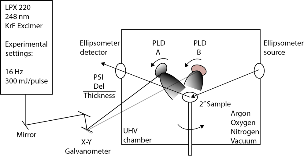 Ellipsometry data were collected in situ using a Woollam M2000, and ellipsometry modeling was performed by using a multilayer model which consisted of a substrate model for silicon, a layer for the oxidation layer that is always initially present on silicon, and a second modeled layer representative of the data collected in situ during the thin film deposition. After a model is generated matching each of the three modeled layers, the film thickness can be calculated. Initial alignment verification and data collection were performed for each sample and the native silicon oxide thickness was calculated to be for each wafer. A model generated parameters defined to constantly fit the data generated during deposition, and the primary parameter of interest for modeling was the real-time thickness. The thickness measured for 100% BN thin film by ellipsometry was 100 nm at completion. Samples were analyzed with a Renishaw inVia Raman microscope, Staib XPS, and Asylum Research MFP3D AFM. 3.Results and DiscussionEllipsometry data were collected for each of four deposition conditions and used to calculate and at five exemplary wavelengths as well as the final film thickness. Table 1 shows the numerical and results at one of the five wavelengths, 632 nm, for each of the experimental conditions. The ellipsometer model used contains three layers: the first layer is an infinitely thick silicon substrate, the second layer is the native silicon oxide layer, and the third layer is a dynamic model of the grown thin film. The silicon substrate and native oxide were measured prior to deposition process and were assumed to remain unchanged. The parameters shown in Table 1 were calculated using a Tauc-Lorentz model, due to its ability to accurately characterize the optical behavior of amorphous materials, including carbon and various nitrides.9–11 Throughout the deposition process, raw psi () and del () data were analyzed within the J.A. Woollam CompleteEase software package using a Cauchy model because of its simplicity and small mean squared error. Numerical components of the model were continuously optimized to approximate and across the wavelength range of the device. The thickness of the growth layer was both calculated and displayed every 8 s. Table 1Ellipsometer summary of film growth on Si wafer with ∼2.25 nm oxide layers.
3.1.XPS CharacterizationXPS characterization was performed on each sample using a Staib XPS system consisting of an ion pump, x-ray source, and energy analyzer. Samples were loaded into an antechamber with a base pressure of or better. The samples were then transferred into the analysis chamber which had a base pressure of . XPS data were collected using a pass energy of 20 eV. All spectra were background corrected using a Shirley background subtraction. Component curves were fitted to each spectrum using a Levenberg−Marquardt algorithm that minimizes , Fig. 2. Each component curve consists of a convolution of Gaussian and Lorenztian functions. Photoemission intensities were corrected to account for Scofield cross sections, kinetic energy, and analyzer transmission function. XPS data were collected with a standard Mg (1253.6 eV) excitation source. The energy scale was calibrated against Au and Cu at the binding energies of 84.0 and 932.6 eV, respectively. The XPS resolution was determined by the FWHM of the Au line, which was found to be 1.2 eV. Fig. 2X-ray photoelectron spectroscopy (XPS) showing boron opposite of carbon for desired BN:C ratio. Both sets of stacked spectra consist of raw data (black), fitted components (blue), and sum curves (red).  Table 2 shows the binding energy () for boron and carbon (B and C ). The normalized concentration of each element is equal to the measured intensity divided by the instrument sensitivity factor for that element. The resulting percentage of the normalized concentration for each element is then the atomic percent. Table 2 shows the surface characterization measurements for the 50% C-50% BN sample. Oxygen contamination, O peak, is shown as being some 28%; this is expected due to the fact that the samples have been exposed to air and were exposed to an ion beam for a brief time before sampling. The same measurement and analysis techniques were used on each of the four samples. Table 2 shows that the ratio of B to C is approximately slightly and the ratio of B to N is just under 1.7. Table 2X-ray photoelectron spectroscopy surface characterization of 50% carbon–50% BN sample. Measurement error is ±0.1 atomic %.
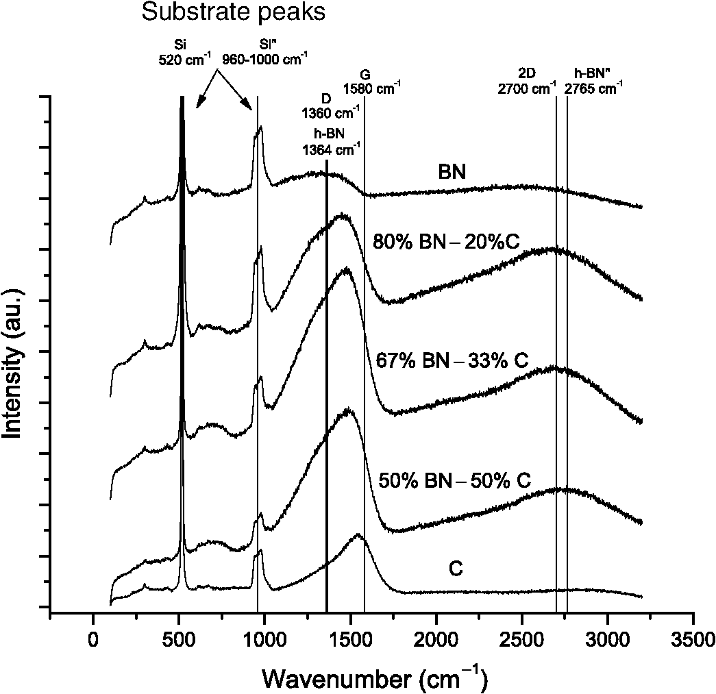
Figure 2 shows plots of the binding energies for boron and carbon 1s peaks. The spectra show cross-contamination that occurred during growth, and are obvious for the first growth of 100% BN, i.e., a laser pulse of carbon would place small amounts of carbon onto the BN target, and pulse onto the BN target would contaminate the carbon target. This issue has been largely resolved with the addition of a shutter over the sample as well as a shield between the two PLD targets which provides for the ability to operate the ellipsometer even while the shutter is closed with PLD operating for the purposes of precleaning the targets, and has been shown to be required. Figure 2 shows the composition summary of B, C, and N for each of the four films deposited and the corresponding XPS composition. The nitrogen content is lower than boron content for each sample, which can be explained by the fact that ionization and atomization of the BN target during the PLD process in vacuum results in a loss of nitrogen. Since the pressure was constant, HV, it was also expected that the same boron to nitrogen ratio will essentially be maintained regardless of BN:C ratio of growth, as shown in Fig. 3, and the ratio is for XPS characterized samples. Fig. 3XPS and EDX summary of ratio (atomic %) and ratio for each setpoint of carbon target pulses (%). 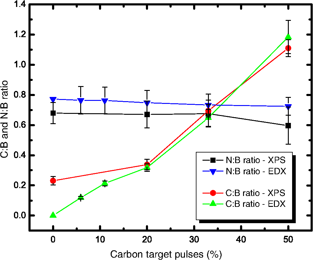 The desired growth setpoints that were also characterized by XPS were BN: 100%, BN: 80%, BN: 67%, and BN:50%, but as is shown in Fig. 3, the actual boron to carbon ratios ended up being 4.33, 2.96, 1.44, and 0.901, respectively. The ratio of boron to nitrogen ended up being 1.472, 1.493, 1.480, and 1.678, respectively. This represents ratios on the order of , , as well as two samples with a ratio near unity, i.e., one sample rich in boron and the other rich in carbon. As was previously mentioned, the four samples grown without mechanical shielding between targets and characterized by XPS show approximately a ratio of boron to carbon for the first sample which should not have had any significant amount of carbon. This error can be from either XPS measurement technique due to air exposure, or due to contamination occurring during the deposition process. Contamination can occur by the fact that if the targets are not physically separated using mechanical shielding, then each laser pulse will have material both deposited on the substrate, but also onto the other laser target and thereby skewing the desired deposition parameters and potentially creating particulates. To test this, six additional samples were grown to approximately 1 μm in thickness with mechanical shielding added between PLD targets to prevent cross-contamination. Energy dispersive x-ray characterization was performed with a Hitachi 3000 tabletop SEM with energy-dispersive X-ray spectroscopy (EDX) attachment. As shown in Fig. 3, the results were virtually identical within the error in terms of composition. However, the first XPS sample shown with a ratio of demonstrates the first sample was contaminated as the EDX sample shows a carbon content of zero as expected, Fig. 3. PLD results in a direct stoichiometric transfer of material from target to substrate, but in vacuum also in all directions, hence the need to have a shield between targets to prevent cross-contamination. Adding a mechanical shield prevented cross-contamination issues. When depositing from the BN target, there is a loss of nitrogen (Fig. 3, ratio below 1) due to the fact that the deposition is being performed in vacuum, which is typical for multielement targets containing nitrogen or oxygen. One of many techniques to raise the resulting thin film nitrogen content is to perform depositions at a pressure of a few Pa of nitrogen. Figure 3 demonstrates that the composition, ratio, can be adjusted with precision using PLD, but optimization process with regard to would need to be performed to obtain the desired nitrogen content as well. For single element targets, it is clear that subnanometer mixing can be accomplished using sequential laser pulses on each target. 3.2.Raman CharacterizationFigure 4 shows four Raman spectra corresponding to each of the four samples and a carbon sample for the reference. A Renishaw inVia Raman microscope having a 514 nm laser excitation and microscope objective was used for the measurements in a confocal mode providing a measurement depth of approximately 1 μm. The peaks shown in each of the spectra below are from the Si substrate and corresponding native oxide layer of ( thick). The carbon sample was deposited with the same conditions as the other four, but for a much shorter period of time yielding a film thickness of , and as such the Si and peaks are much larger than those observed in the other samples. Raman spectra of carbon are expected to have a D peak at and a G peak at , and boron nitride is expected to have Raman peaks at for cubic BN (c-BN) and for hexagonal BN (h-BN).12 As is shown in Fig. 4, the spectra above are as could be expected, essentially a D peak component, a much larger G peak component, and second harmonic of the D peak. By peak fitting the D and G components using two Gaussian functions, for pure carbon, the algorithm returns that there is dominantly graphitic carbon having a G peak centered at and a much smaller D peak centered at , and for the pure BN sample, there is only h-BN with a broad peak centered around . The D peak and h-BN peak overlap and the peak position of their summation shifts lower in wavenumber with the increasing BN content. Since the depositions were performed without a heated substrate c-BN was not expected to be formed, which is confirmed by the absence of a peak. The spectra in Fig. 4 for 80% BN-20% C deposited by PLD are equivalent to the Raman spectra presented in Ref. 13 from sputtering of in 10% to obtain a film composition of 48% B, 12% C, and 40% N.13 Beginning with the pure carbon sample Raman spectra, increasing the amount of BN causes the G peak to be reduced relative to the h-BN peak as the boron content is increased, and hence the h-BN peak of is increased in intensity. The broad peak around is the second harmonic of the peak. The second harmonic of bulk h-BN (h-BN′′) is represented by a broad peak at , while the BN thin film second harmonic is , Fig. 4.14 One noticeable detail is that with each of the four films having approximately the same thickness, the pure BN film has a Raman intensity at , which is much smaller than the substrate related to peak intensity at . This lack of Raman response for pure BN would imply that either the film is not nearly as thick or that BN is perhaps much more transparent to 514 nm laser excitation than carbon. The film thickness was verified with ellipsometer modeling, AFM, and a KLA Tencor profilometer, so the lack of response must be from the actual material properties such as the absorption coefficient at 514 nm. 3.3.AFM CharacterizationAn MFP3D AFM (Asylum Research) was used to measure film thickness and surface root-mean-squared (RMS) roughness for each sample composition. The data shown in Fig. 5 were acquired in ac (tapping) mode by an Olympus ac160 silicon probe with a nominal tip radius of . Sample thickness was measured relative to the silicon substrate (disregarding an uneven edge formed by the removal of a mask adjacent to the deposited film). A measured thickness of 103.7 nm is indicated by the cross section in Fig. 5(a) for a BN-50:C-50 scan. An image analysis function in the MFP3D (Igor Pro-based) software was used to calculate the RMS roughness of unmodified topography data according to , where is the total number of height values. Figure 5(b) shows a representative 10 μm scan of BN-80: C-20, which yielded a full image RMS value of 7.87 nm. RMS values were on the order of 7 to 11 nm for randomly sampled 10 μm areas. The horizontal lines in Fig. 5(b) were artifacts from the instrument of the tallest features in the scan line. The particulates captured in Fig. 5(b), displayed as white spots, were observed for each sample composition and could be attributed to the deposition of material onto the opposing PLD target with the ablation pulse. Each focused laser pulse was approximately , with each target material having some 45-mm diameter active area of ablation, allowing buildup of particulates from many pulses onto each opposite target before an actual deposition pulse. In this manner, some degree of particulates are expected, but could be mitigated with the addition of a shield between the laser targets.15 Fig. 5Atomic force microscopy (AFM): (a) height profile across the edge of a BN-50:C-50 sample indicates approximate 100 nm film thickness relative to the silicon substrate. The uneven edge morphology was formed by the removal of a mask after deposition. (b) Representative 10 μm BN-80:C-20 surface scan yields 7.9 nm RMS roughness. RMS values were to 11 nm over randomly sampled 10 μm areas, and the surface morphology is typical for the four compositions evaluated. Particulate heights range between and ; horizontal lines across the tallest features are AFM scanning artifacts. 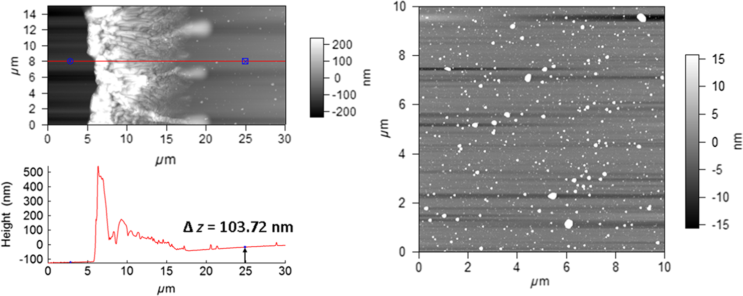 3.4.In Situ Ellipsometer CharacterizationIn situ ellipsometer data were collected for each of the four depositions, with the 50% BN–50% C and the 80% BN–20% C deposition dynamic data being shown in Fig. 6. Each deposition lasted approximately 15 min, with the deposition conditions being pulse, and a 16 Hz pulse rate from the laser. During the deposition, the growth rate of the thin film thickness was linear as shown in Figs. 6(c) and 6(d). The value of changed significantly during growth with each associated wavelength. The effect of different composition of materials and the difference in optical property of the material was significant, with the 80% BN–20% C having the largest change in the magnitude of . The change in is most pronounced at 371.3-nm wavelength, Figs. 6(a) and 6(b). Fig. 6Dynamic ellipsometer spectra collected during deposition: (a) BN-50:C-50 and (b) BN-80:C-20. In situ thickness modeled using ellipsometry (c) for BN-50:C-50 and (d) for BN-80:C-20.  The ellipsometer measures psi and del across the wavelength range of 370 to 1690 nm. CompleteEase software from J.A. Woollam provides for definition of optical layers, and in this case, a modeled layer for the Si wafer substrate, the native oxide layer, and a Cauchy model for each thin film of interest. Each optical layer is parameterized by the thickness, and , and an appropriate model such as Tauc-Lorentz, Sellmeier, or in the simplest form Cauchy for transparent materials. The CompleEase software iteratively fits all measurements to all of the defined model layers to determine optimal model parameters. The Cauchy model, Eqs. (1) and (2), is an approximate function of the Sellmeier model in which a series expansion is used to compute and : In Eq. (1), the constant represents the approximate index of refraction and together with and define the index dispersion. Band edge is a parameter in nanometers that is set manually, whereas the and paramters determine the shape of the extinction coefficient dispersion. Once the best fit of the parameters , , , , and are obtained by CompleteEASE, where and and thickness are calculated. From a Cauchy model fit of the psi and del in situ data of two deposition conditions, and were calculated at five representative wavelengths for the 50% BN–50% C and 80% BN–20% C cases, Fig. 7. The 50% BN case shows that particular film is very absorptive, especially at 514 nm where strong Raman spectra were collected, and the 80% BN case was not nearly as absorptive, Fig. 7. The extinction coefficient for pure BN, Fig. 7, was closest to zero at 514 nm as compared to the others, and was correspondingly the weakest Raman scattering thin film at , Fig. 4. Fig. 7(a) and (b) with the wavelength for pure BN and samples having tuned stoichiometry in thickness and C thick. 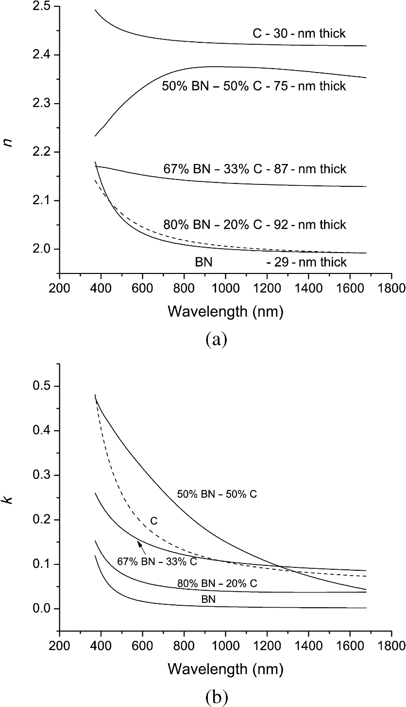 Additionally, all samples and values are shown in Fig. 7: pure BN, 80% BN–20% C, 67% BN–33% C, 50% BN–50% C, and pure carbon. BN has the lowest value of index of refraction of the films grown at 2.0, and carbon the highest around 2.4.15 As demonstrated in Fig. 7, changing the stoichiometry by adding amounts of carbon will cause a shift in the actual optical properties of index of refraction and absorption coefficient, which can be desired for filters, optical lenses, coatings, metamaterials, or other applications. Increasing carbon concentrations, Table 3, show that when compared at a specific wavelength such as 632 nm, the and values increase in an increasing fashion. As the carbon concentration is linearly increased from 0 to some 41 atomic %, the index of refraction increases from 2.03 to 2.36 at 632 nm and the value of increases from to . Typical values of index of refraction for h-BN are 1.8 and 3.3 for . Table 3Changes of n and k according to carbon concentration at 632 nm.
4.ConclusionsNanotechnology research requires the ability to fabricate and test many different material samples having defined, functionally graded, or static material properties or features at the 1 to 100 nm scale. PLD is a highly energetic and efficient technique to create thin film materials, but typically allows for only stoichiometric transfer of material from a single target material to substrate. As was demonstrated, using more than one physical target and programming a desired number of laser pulses onto each laser ablation target using a galvanometer resulted in a thin film material which had tailorable subnanometer mixing throughout the thin film from two exemplary pure target materials: BN and C. Typically, some 150 pulses at from the excimer laser resulted in 1 nm of material being deposited, demonstrating that island growth must occur on a per pulse basis. By calibration of the number of laser pulses per target to XPS or EDX composition ratios, any desired linear combination of B:C or other pure target materials can be achieved. By modeling the carbon content and the resulting index of refraction, a film containing a desired index of refraction (at 632 nm) between 2.02 and 2.36 could be deposited using this deposition technique. The amorphous nature and change of response with composition of each of the materials were verified using Raman spectroscopy. AFM can be used to measure the thickness, grain size, and RMS roughness of a sample, with typical roughness being shown to be on the order of 11 nm for samples which were not biased nor heated during deposition. Optical ellipsometry in situ was shown to be able to model the thickness of multiple layers, any combination of laser pulses, and all in real time while the laser is operating growing a film. Optical ellipsometry allows for all wavelengths from 370 to 1690 nm to be characterized simultaneously while depositing a thin film, and allows for the implementation of process control to be able to deposit thin films having specific thicknesses or optical properties, as is required for optical metamaterials, thermal materials, and nanotechnology applications. AcknowledgmentsThe authors thank the Air Force Office of Scientific Research for financial support. Adam Waite and Art Safriet are thanked for helping the develop target and substrate holding mechanisms, Kurt Eyink for ellipsometry advice and analysis, and Michael Marciniak, Andrey Voevodin, and David Zelmon for several useful discussions. R.J. was instrumental in ellipsometry procurement and implementation and optics train for excimer. P.T.M. aided in chamber design. N.R.M. was involved in experimental apparatus implementation. L.S. conducted ellipsometric analysis of samples. T.C.B. performed XPS. J.L.R. performed AFM. M.A.L. researched BCN details. J.G.J. developed the overall apparatus design, authored deposition software, developed synchronization of the laser pulses to the optical mirror system, performed thin film growth with in situ ellipsometry measurements, and Raman and EDX characterization. ReferencesT. Zehnderet al.,
“Determination of limits in deposition of adhering a-C films on silicon produced by pulsed laser deposition,”
Thin Solid Films, 263
(2), 198
–202
(1995). http://dx.doi.org/10.1016/0040-6090(95)06582-2 THSFAP 0040-6090 Google Scholar
A. Perroneet al.,
“Boron carbonitride films deposited by pulsed laser ablation,”
Appl. Surf. Sci., 133
(4), 239
–242
(1998). http://dx.doi.org/10.1016/S0169-4332(98)00207-4 ASUSEE 0169-4332 Google Scholar
K. Raidongiaet al.,
“Synthesis, structure, and properties of homogeneous nanotubes,”
J. Mater. Chem., 18
(1), 83
–90
(2008). http://dx.doi.org/10.1039/b712472d JMACEP 0959-9428 Google Scholar
D. BlankH. Rogalla,
“In-situ diagnostics at high pressures: ellipsometric and RHEED studies of the growth of ,”
Mater. Res. Soc. Symp. Proc., 502 237
–247
(1997). http://dx.doi.org/10.1557/PROC-502-237 MRSPDH 0272-9172 Google Scholar
G. E. Jellison,
“Spectroscopic ellipsometry data analysis: measured versus calculated quantitites,”
Thin Solid Films, 313–314
(1), 33
–39
(1998). http://dx.doi.org/10.1016/S0040-6090(97)00765-7 THSFAP 0040-6090 Google Scholar
Md. Mannanet al.,
“Atomic arrangement, composition and orientation of hexagonal BCN films synthesized by radiofrequency plasma enhanced CVD,”
J. Ceram. Soc. Jpn., 117
(1364), 503
–507
(2009). http://dx.doi.org/10.2109/jcersj2.117.503 JCSJEW 0914-5400 Google Scholar
J. G. JonesA. A. VoevodinJ. S. Zabinski,
“Characterization of plume fluence for laser ablation of yttria stabilized zirconia in mixed oxygen and argon environments,”
Surf. Coat. Technol., 146
(1), 258
–262
(2001). http://dx.doi.org/10.1016/S0257-8972(01)01473-6 SCTEEJ 0257-8972 Google Scholar
A. Gorbunovet al.,
“Formation of unusual intermetallic phases by vacuum PLD,”
Appl. Surf. Sci., 197–198
(1), 475
–480
(2002). http://dx.doi.org/10.1016/S0169-4332(02)00374-4 ASUSEE 0169-4332 Google Scholar
G. E. JellisonF. A. Modine,
“Parameterization of the optical functions of amorphous materials in the interband region ,”
Appl. Phys. Lett., 69
(3), 371
–373
(1996). http://dx.doi.org/10.1063/1.118064 APPLAB 0003-6951 Google Scholar
G. E. Jellisonet al.,
“Characterization of pulsed-laser deposited amorphous diamond films by spectroscopic ellipsometry,”
Mater. Res. Soc. Symp. Proc., 526 349
–354
(1998). http://dx.doi.org/10.1557/proc-526-349 MRSPDH 0272-9172 Google Scholar
V. I. Merkulovet al.,
“Structure and optical properties of amorphous diamond films prepared by ArF laser ablation as a function of carbon ion kinetic energy ,”
Appl. Phys. Lett., 73 2591
–2593
(1998). http://dx.doi.org/10.1063/1.122515 APPLAB 0003-6951 Google Scholar
S. Reichet al.,
“Resonant Raman scattering in cubic and hexagonal boron nitride,”
Phys. Rev. B, 71 205201
(2005). http://dx.doi.org/10.1103/PhysRevB.71.205201 PRBMDO 1098-0121 Google Scholar
A. LousaJ. EsteveS. Muhi,
“BCN thin films near the B4C composition deposited by radio frequency magnetron sputtering,”
Diamond Relat. Mater., 9
(3–6), 502
–505
(2000). http://dx.doi.org/10.1016/S0925-9635(99)00319-2 DRMTE3 0925-9635 Google Scholar
L. Songet al.,
“Large scale growth and characterization of atomic hexagonal boron nitride layers,”
Nano Lett., 10
(8), 3209
–3215
(2010). http://dx.doi.org/10.1021/nl1022139 NALEFD 1530-6984 Google Scholar
E. Frankeet al.,
“In situ infrared and visible-light ellipsometric investigations of boron nitride thin films at elevated temperatures,”
J. Appl. Phys., 84
(1), 526
–532
(1998). http://dx.doi.org/10.1063/1.368083 JAPIAU 0021-8979 Google Scholar
BiographyJohn G. Jones received the BS EE from Rose-Hulman Institute of Technology and the PhD from the University of Cincinnati. He is a senior materials research engineer for the USAF at the AFRL in the Materials and Manufacturing Directorate. Past research collaborations included process development of PLD processing of YBCO superconductors, HiPco for SWNT at Rice University, electronics for the MISSE-7 program, and thermal management materials. Current research focuses on PVD of thin films for nanoelectronics. Lirong Sun received the PhD degree in the electro-optics graduate program from the University of Dayton, Ohio, in 2009. She is currently a senior scientist at General Dynamics Information Technology, working at the Air Force Research Laboratory. Her research interests are thin film coatings and characterizations of optical and structural properties of composited materials for optical thin film coatings and metamaterials applications. Neil R. Murphy is currently a PhD student in materials engineering at the University of Dayton. He has been working within the Materials and Manufacturing Directorate at Wright Patterson Air Force Base since 2010, where his primary focus is on the deposition and characterization of optical thin films. Tyson C. Back received the PhD in materials engineering from University of Dayton. He currently works for the Materials and Manufacturing Directorate at Wright-Patterson Air Force Base. His work at Wright-Patterson involves the characterization of carbon nanotube field emission cathodes. In addition to field emission measurements, surface analysis techniques are used to determine the surface chemistry and electronic structure of the cathodes before and after thin film deposition of low work function coatings. Matthew A. Lange is a graduate of the Air Force Institute of Technology in applied physics. He has over 14 years’ experience in experimental physics and mathematical modeling as applied to chemical kinetics, thin film deposition, material diagnostics, optical spectroscopy, plasma spectroscopy, electrodynamics, laser systems, directed energy effects, and plasma physics. He also authored or coauthored several journal articles, technical reports, and conference papers. Jessica L. Remmert received the BS degree in physics-engineering from Washington and Lee University in 2005 and the MS degree in mechanical engineering from Georgia Institute of Technology in 2007. Her graduate level and subsequent research at the Air Force Research Laboratory’s Materials and Manufacturing Directorate, Thermal Sciences Branch (WPAFB, Ohio) has emphasized the use of atomic force microscopy to characterize materials. P. Terrence Murray received the PhD in physical chemistry from University of North Carolina (Chapel Hill) in 1979 and was a Welch Postdoctoral Fellow at the University of Houston until 1982, when he joined the University of Dayton (UD) Research Institute. He has over 25 years of experience in laser materials processing and holds a joint appointment as professor in the Graduate Materials Engineering program at UD. Rachel Jakubiak is currently employed by the U.S. Air Force Research Laboratory (AFRL) where she investigates materials and optical properties of vacuum deposited thin films. While at AFRL her research areas have included random lasing, switchable polymer lasers, nonlinear optical measurements of third-order phenomenon, and multilayer coatings for optical band control. In 2012, she was elevated to senior membership status in SPIE and since 2007 has cochaired an SPIE conference on organic photonic materials. |