|
|
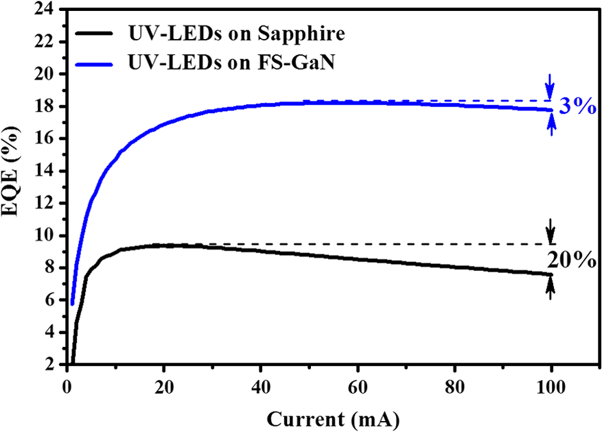
1.IntroductionThe 350 to 400 nm InGaN-based ultraviolet light-emitting diodes (UV-LEDs) have received enormous attention for practical applications, such as biosensors, high density storage, and short-distance optical fiber communications.1–3 In addition, the white-light LEDs can be realized by using InGaN-based UV-LEDs chip excited the phosphor of red, green, and blue (RGB).4–6 Compared with the case of white-light emission from blue LEDs chip coated with yellow phosphors, many researches pointed out that has many excellent properties, such as lower wavelength shift as increasing injection current, high luminous efficiency, white point determined by phosphor only, better color rendering and stable light color.7 Nevertheless, there is still lack of a suitable substrates for InGaN-based UV-LEDs devices to fully develop their advantages. Typically, InGaN-based UV-LEDs were grown on sapphire by hetero-epitaxial techniques, such as metal-organic chemical vapor deposition (MOCVD).8,9 However, the epitaxial layer of InGaN-based UV-LEDs still contains a high defect density (around to ) and large strain-induced piezoelectric field due to the large lattice mismatch and the difference in thermal expansion coefficients of GaN-based films and sapphire substrates, resulting in the reduction in the internal quantum efficiency (IQE) of InGaN-based UV-LEDs devices. On the other hand, the external quantum efficiency (EQE) decreases drastically below the wavelength of 400 nm.10 It is well known that in low indium content InGaN quantum wells (QWs), an AlGaN barrier is necessary for carrier confinement. But the two materials of AlGaN and InGaN are very different in growth temperature, which strongly affects strongly the quality of material and device performances. In order to overcome the above mentioned problem, our group has replaced the AlGaN barrier with an InAlGaN quaternary material in an InGaN/AlGaN multiple quantum wells (MQWs) system, which demonstrated an improvement of 55% in output power and a droop of 13% in efficiency.11 Additionally, it is believed that the optical and electrical properties of InGaN-based UV-LEDs were very sensitive to the defect density in the epilayer, suggesting a high crystalline quality epilayer could dramatically improve the device’s performance.12,13 The recent availability of free-standing GaN (FS-GaN) substrates with a low defect density (about ) could perhaps facilitate this development, which can enhance the light output power, the IQE, and the EQE of InGaN-based UV-LEDs.14–16 In order to further improve the performance of the UV-LEDs with InGaN/InAlGaN MQWs devices, in the present study we will introduce a FS-GaN substrate for the homo-epitaxial growth of high quality InGaN-based UV-LEDs devices with InAlGaN quaternary barrier. In addition, the effects of the FS-GaN substrate on the InGaN-based UV-LEDs grown by atmospheric pressure metal-organic chemical vapor deposition (AP-MOCVD) are systematically analyzed. Detailed analyses of the grown InGaN-based UV-LEDs will be demonstrated, and electro-optical properties of the UV-LEDs based on a FS-GaN substrate will also be discussed. 2.Experimental ProcedureAll UV-LEDs with an InGaN/InAlGaN MQWs epitaxial structure were grown using a commercial AP-MOCVD system (Model: Nippon SR4000, Japan) with a horizontal reactor in the same run. The MO compounds of TMGa, TMIn, TMAl, and gaseous were employed as the reactant source materials for Ga, In, Al, and N, respectively, and and were used as the carrier gases. The substrates employed here were 2-inch FS-GaN substrates with a thickness of 300 μm, which were provided by Sumitomo Electric Industries, Ltd., in Japan and was manufactured from GaAs substrates.17 The epitaxial structure of the UV-LEDs investigated is depicted in Fig. 1, comprising a 2.5-μm-thick n-GaN epilayer grown at 1150°C, a ten-period InGaN/InAlGaN MQWs active layer grown at 830°C, 15-nm-thick Mg-doped and 10-nm-thick Mg-doped electron-blocking layers were grown at 1030°C, a 55-nm-thick p-GaN layer was grown at 1030°C, and a 5-nm-thick p-InGaN contact layer was grown at 830°C. In addition, the growth of the UV-LEDs with the InGaN/InAlGaN MQWs epitaxial structure on an un-doped GaN/sapphire template was also conducted for comparison. Fig. 1Schematics of ultraviolet light-emitting-diodes (UV-LEDs) with InGaN/InAlGaN MQWs structures grown on free-standing GaN (FS-GaN) substrate.  After epitaxial growth, the indium tin oxide film (180 nm) was first deposited on the UV-LEDs as a transparent contact layer. Then, the surfaces of the UV-LEDs were partially etched until a 1.5-μm depth of the n-GaN layers was exposed. We subsequently deposited Cr/Pt/Au () onto the exposed n-GaN and p-GaN layers to serve as the n-type and p-type electrodes, respectively. Finally, the UV-LEDs were cut into square pieces with dimensions of . The crystalline quality and interface of our epitaxial structures were evaluated by high-resolution double-crystal x-ray diffraction (HRDCXD D8) using radiation as the x-ray source (). Room temperature Raman scattering was used to analyze the residual strains of the GaN epitaxial layers and UV-LEDs. The distribution and threading behaviors of dislocations in the epilayer were then studied by transmission electron microscopy (TEM). Moreover, the interfacial microstructures of the epilayer were observed by high-resolution TEM (HRTEM). The optical properties were investigated by electroluminescence measurements performed at room temperature. Finally, the light-current-voltage (L-I-V) characteristics of the UV-LEDs devices were measured at room temperature under continuous-wave (CW) operation. 3.Results and DiscussionFigure 2 shows the HRDCXD rocking curves in the (0002) and the () reflections, obtained from the UV-LEDs grown on the FS-GaN and sapphire substrates. The full widths at half maximum (FWHM) of the UV-LEDs on the FS-GaN substrate are only 83 arc sec for (0002), and 77 arc sec for (), respectively. Both the FWHM values of the UV-LEDs on the FS-GaN substrate are narrower than that of UV-LEDs on a sapphire substrate by a factor of 4 to 5. In wurtzite GaN-based films, the FWHM of the (0002) rocking curve is associated with the density of the screw or mix dislocations, whereas the FWHM of the () rocking curve is affected by all dislocations.18 Therefore, we can calculate the total defect density with the formula from Ref. 19. The calculated total defect density is about for the UV-LEDs on the sapphire substrate and for the UV-LEDs on the FS-GaN substrate. This result shows that the defect density of the UV-LEDs can be reduced dramatically by introducing FS-GaN as a substrate for epitaxy of InGaN/InAlGaN MQWs UV-LEDs. In addition, it is clear that the rocking curves in the (0002) and the () reflections contain the additional peaks by Gauss function, in which peak 1 is 72.01 arc sec for (0002) and peak 2 is 48.44 arc sec for (), in addition to that of the main peak of the FS-GaN substrate, respectively. These additional peaks that are peak 1 and peak 2 in the (0002) and the () reflections, respectively, correspond to the internal structural grain boundary20 with a very low angle (tilt angle ), where tilt angle of peak 1 is 72.01 arc sec for (0002) and for peak 2 is 48.44 arc sec for () by Gauss function from the adjoining regions, respectively. The HRDCXD results were attributed to the hexagonal inverse pyramidal pits which are constructed by facets of the FS-GaN substrate.17 Fig. 2High-resolution double crystal X-ray diffraction (HRDCXD) rocking curves of UV-LEDs grown on FS-GaN and sapphire substrate in the (a) (0002) and (b) () reflection. 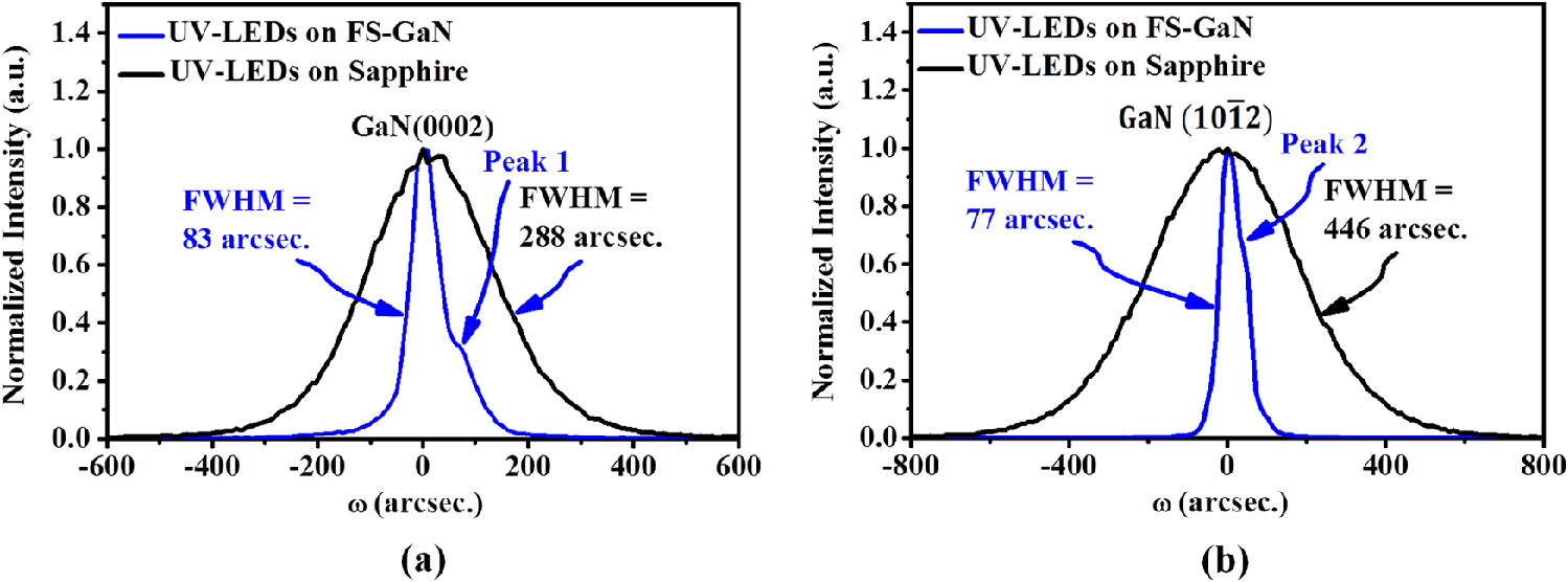 Figure 3(a) shows the HRDCXD scan for the UV-LEDs epitaxial structures grown on the FS-GaN and sapphire substrates. As can be seen, all the HRDCXD patterns demonstrate periodical structures, which can be attributed to the InGaN/InAlGaN MQWs that were grown. The strongest peak is due to the GaN layer and the spectra for the UV-LEDs on the FS-GaN substrate clearly show high-order InGaN/InAlGaN MQWs diffraction peaks with the fourth-order satellite peak still being observable, indicating good layer periodicity. In addition, the InGaN/InAlGaN MQWs period can be determined from the positions of the InGaN/InAlGaN MQW satellite peaks. This suggests that the specimen of the UV-LEDs on the FS-GaN substrate also has abrupt interfaces between the InAlGaN barrier and the InGaN well. The interface roughness (IRN) of the InGaN/InAlGaN MQWs structures grown on the FS-GaN substrate was further analyzed by using the following equation:21,22 where is the order of the satellite; and are the periods of satellite peak and IRN, respectively; is the angle distance between adjacent satellite peaks; and and are the FWHM of the zeroth- and ’th-order peaks, respectively.Fig. 3(a) (0002) reflection HRDCXD curves of UV-LEDs grown on FS-GaN and sapphire and (b) the full widths at half maximum of satellite peak in InGaN/InAlGaN MQWs as a function of the order of the satellite peak.  Figure 3(b) shows the FWHM of the satellite peak in InGaN/InAlGaN MQWs as a function of the order of the satellite peak. As can be seen, the IRN of the UV-LEDs on a sapphire substrate is about 5.16%. However, the IRN can further be reduced to 1.55% with the UV-LEDs grown on the FS-GaN substrate. As indicated in Ref. 21, the IRN of MQWs is affected by the defects, microstructure, and phase separation in MQWs. Therefore, our x-ray analysis results might indicate that the crystalline quality of the InGaN/InAlGaN MQWs epitaxial structure grown on the FS-GaN substrate is superior to those grown on sapphire substrates. It was well known that the traditional InGaN-based UV-LEDs exhibited large biaxial strain due to a large lattice-mismatch and thermal expansion coefficient incompatibility between the GaN epilayer and sapphire, resulting in a large piezoelectric field along the c-plane orientation, thus forming the quantum confined Stark effect in the MQWs which leads to the reduction in light output power and recombination rate for the electron and hole. As the c-plane FS-GaN substrate manufacturing from the GaAs substrate that will exhibite lower lattice-mismatch and less difference of thermal expansion coefficient17 than the FS-GaN substrate manufacturing from sapphire by hydride vapor phase epitaxy,23,24 the less residual stress in the FS-GaN substrate manufacturing from the GaAs substrate may be obtained. Thus, in this paper, we have used a complementary method for residual stress measurement, specifically Raman spectroscopy. The residual stress measurement using Raman spectroscopy is based on the peak position shift of observable Raman modes, which is directly proportional to the lattice-strain. Figures 4(a) and 4(b) show the Raman spectrum for the UV-LEDs grown on the sapphire and the FS-GaN substrates. The Raman spectra show two Raman shift peaks: one can be attributed to the (high) mode of the GaN epilayer and the other can be attributed to the [longitudinal optical (LO)] mode of the GaN epilayer. The A1(LO) of Raman active modes refers to Ref. 25. According to the Harima26 report, the (high) mode gives atomic displacement perpendicular to the c-axis, while the other (LO) mode gives atomic displacement along the c-axis. Although two optical photon modes, (high) and (LO), are observed in the c-plane GaN epilayer back-scattering according to the selection rules, our study selected the nonpolar (high) photon mode to estimate the residual stress due to its sensitivity to strain in the basal plane (c-plane) and also directly to the in-plane residual stress in the (0001)-oriented GaN epilayers. The Raman shift peaks of (high) for UV-LEDs grown on FS-GaN and sapphire substrates shown in Fig. 4(c) were located at around 567.2 and , respectively. We can calculate the strain value of the InGaN/InAlGaN MQWs by the following equation.25 where is the Raman shift peak difference between the strained GaN epilayer and the strain-free GaN epilayer. The calculated in-plane compressive stress () was about 0.31 and 1.12 GPa for UV-LEDs grown on the FS-GaN and sapphire substrate, respectively. In other words, the InGaN-based UV-LED was grown on the FS-GaN substrate using a homo-epitaxial technique, i.e., the FS-GaN substrate can help the recombination rate of electron and hole and thus the light output power is expected to rise. Hence, the results from the Raman analyses are in good agreement with those presented by the studies of electric properties as described below.Fig. 4Room temperature (RT) Raman spectrum for UV-LEDs grown on (a) sapphire and (b) FS-GaN substrates. (c) The residual stress based on the peak position shift of observable Raman (high) modes. 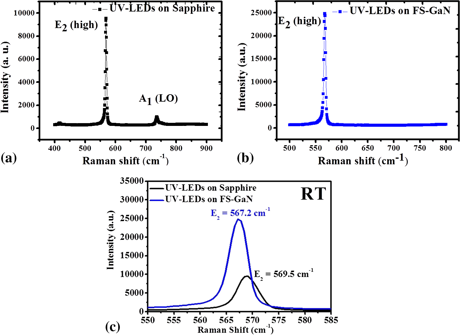 On the other hand, we used TEM to investigate the crystalline quality of the UV-LEDs grown on the FS-GaN and the sapphire substrates. In other words, the two-beam TEM images will be used for quantifying the nature and density of defects. Heying et al.18 pointed out that the pure edge and the mixed defects can be visible under a two-beam condition; the pure screw and the mixed defects can be visible under a two-beam condition. In our case, Figs. 5(a) and 5(b) show bright field scanning TEM images for UV-LEDs grown on sapphire and FS-GaN substrates, respectively. In addition, the two-beam TEM images were taken, as shown in Figs. 5(c) and 5(d) for the UV-LEDs on the sapphire, and in Figs. 5(e) and 5(f) for the UV-LEDs on the FS-GaN. When UV-LEDs were grown on sapphire, we clearly find that the epilayer of the UV-LEDs grown on the sapphire exhibited many edges, screws, and mixed defects. In addition, the defects can be seen radiating vertically from the interface between the GaN-based epilayer and sapphire into the InGaN/InAlGaN MQWs region and the p-AlGaN layer, as shown in Figs. 5(c) and 5(d). Therefore, quite a large number of defects were presented in the whole film on the sapphire substrate, as shown in Fig. 5(a). From Fig. 5(a), the edges, screws, and mixed defects were estimated to be , , and , respectively, which led to a total defect density of about . However, when the substrate for the epitaxy of the UV-LEDs was changed from sapphire to FS-GaN, it can be clearly seen that the crystallography of the UV-LEDs epilayer was drastically different from that of UV-LEDs epilayer on a sapphire substrate. No edges, screws, and mixed defects were observed throughout the observed area. As shown in Figs. 5(b), 5(e), and 5(f), the total defect density including edges, screws, and mixed types was considered to be or less, which agrees well with our HRDCXD rocking curve data, further proving that homo-epitaxial is an effective measure to improve the crystal quality of UV-LEDs. Fig. 5Bright field cross-sectional transmission electron microscopy (TEM) images from the UV-LEDs on (a) sapphire and (b) FS-GaN substrate. Two-beam TEM images was taken from the UV-LEDs on sapphire [(c) and (d)] and FS-GaN [(e) and (f)], where (c) and (e) dark field cross section, ; (d) and (f) dark field cross section, .  To better understand the effect of defects on the formation of V-shape pits (V-pits) or microstructures or quantum dot (QD) structures of InGaN/InAlGaN MQWs, HRTEM images of the InGaN/InAlGaN MQWs region were obtained, as shown in Fig. 6. As can be seen, the differences for the InGaN/InAlGaN MQWs between the two specimens was relatively large. For UV-LEDs on the sapphire substrate, there are many V-pits created in the MQWs region, as shown in Fig. 6(a). In addition, the microstructures or the QD structures can be clearly observed, and the spacing between these microstructures or QD structures was estimated to be 1 to 2 nm, as shown in Fig. 6(b). However, when the InGaN/InAlGaN MQWs were grown on the FS-GaN substrate, the InGaN/InAlGaN MQWs exhibited a relatively perfect crystalline structure and without any V-pits or microstructures or QD structures to be observed, as shown in Figs. 6(c) and 6(d). The nonuniform distribution of indium and phase separation in the InGaN well was not the main reason for the difference of InGaN/InAlGaN MQWs between the two specimens since they were grown in the same run. The difference of the substrate for epitaxy of the UV-LEDs could be responsible for such a great difference in the InGaN/InAlGaN MQWs between the two specimens since the homo-epitaxial growth of the UV-LEDs on the FS-GaN substrate can reduce the defects in MQWs. In addition, the V-pits or microstructures or QD structures can result in rougher interfaces in InGaN/InAlGaN MQWs. Therefore, comparing the results in Fig. 6 with those in Fig. 5, we can demonstrate that the UV-LEDs with the InGaN/InAlGaN MQWs grown on the FS-GaN substrate exhibited a more orderly structure, better uniformity, and sharper interface due to a reduction in the defects including edges, screws, and mixed types radiating from the interface between the GaN-based epilayer and substrate. Fig. 6High-resolution TEM (HRTEM) images for UV-LEDs on sapphire substrate [(a) and (b)] and FS-GaN [(c) and (d)]. The diffraction condition is g0002.  The LED devices fabricated on the basis of the material structure of UV-LEDs with InGaN/InAlGaN MQWs grown on the FS-GaN and the sapphire substrates were characterized. Figure 7(a) gives the light output power as a function of the forward current for all the UV-LEDs fabricated. Generally, the commercialized UV-LEDs operate at a forward current of 20 mA for chip size. However, as exhibited in Fig. 7(b), the I-V characteristics of the UV-LEDs grown on the sapphire substrate differ somehow from those of the UV-LEDs grown on FS-GaN substrates. Hence, in our case, the light output power of the UV-LEDs was obtained as follows. For the UV-LEDs grown on the FS-GaN and the sapphire substrates, the light output power was obtained under the forward currents of 20 and 100 mA. The light output powers obtained from the UV-LEDs grown on the sapphire substrate are 6.0 mW at 20 mA and 24.3 mW at 100 mA. However, the light output power goes up to 10.8 mW at 20 mA and 57 mW at 100 mA for the UV-LEDs grown on the FS-GaN substrate. In other words, compared to the UV-LEDs grown on the sapphire, the light output power for the UV-LEDs grown on the FS-GaN substrate was improved by 80% at 20 mA and 90% at 100 mA. Evidently, the light output of the UV-LEDs grown on the FS-GN substrate is superior to those grown on sapphire, which helps to further recognize the merit of using the FS-GaN substrate for the fabrication of UV-LEDs. Fig. 7(a) Light output as a function of forward current and (b) I-V characteristics for the UV-LEDs grown FS-GaN and sapphire substrate. All data were obtained under continuous-wave (CW) operation. 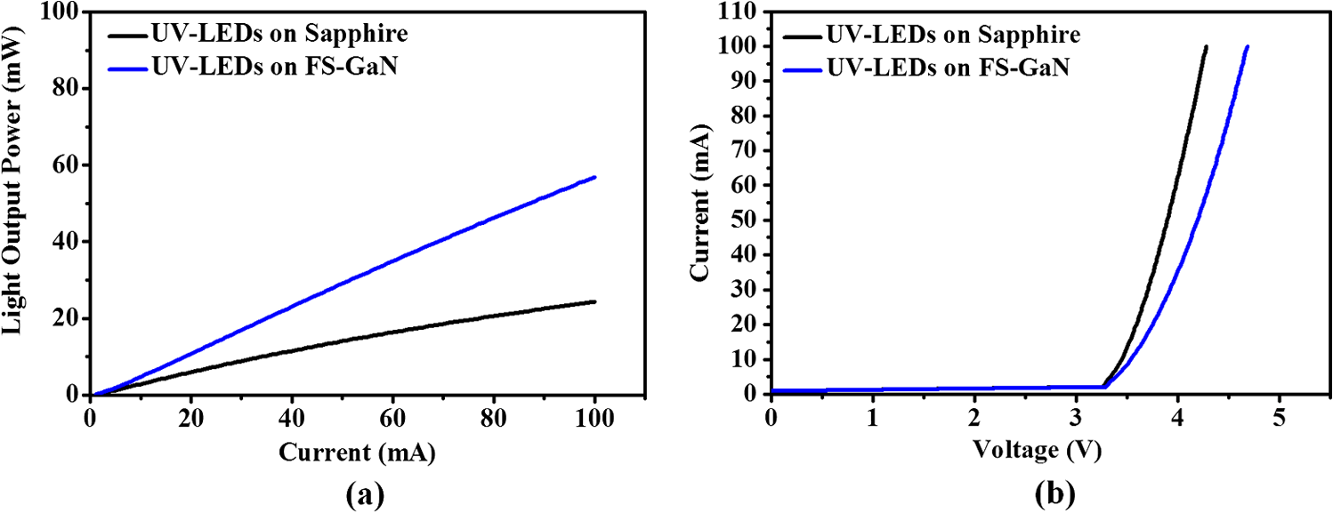 Finally, Fig. 8 shows the EQE as a function of forward current for the UV-LEDs grown on the FS-GaN and the sapphire substrates. The EQE of these two types of the UV-LEDs are under CW operations. The maximum of the UV-LEDs grown on the FS-GaN substrate appear at an injection current of 53 mA, which was much higher than that for the UV-LEDs grown on sapphire substrate (at 20 mA). More interestingly, the efficiency droop, defined as , was reduced from 20% in the UV-LEDs grown on the sapphire substrate to 3% in the UV-LEDs grown on the FS-GaN substrate. Recently, the results of Yu et al.27 pointed out that the lower carrier localization and better uniformity in MQWs will show lower droop behavior. Hence, this significant improvement in efficiency can be mainly attributed to the improvement of crystal quality and uniformity in MQWs and better heat dissipation in the case of the UV-LEDs grown on the FS-GaN substrate. Therefore, the FS-GaN substrates should be a better choice for high power UV-LED applications. 4.ConclusionsIn summary, we have grown UV-LEDs epitaxial structure on the FS-GaN substrates manufactured from a GaAs substrate by AP-MOCVD. The HRDCXD measurements showed that the UV-LEDs structure grown on the FS-GaN substrate exhibited sharp interfaces between the InAlGaN barrier and InGaN well and a uniform QW period of InGaN/InAlGaN. In addition, the IRN of the InGaN/InAlGaN MQWs structure grown on the FS-GaN substrate was estimated to be 1.56%. For crystal quality, the FWHM of the HRDCXD rocking curve in the (0002) and the () reflections were about 83 and 77 arc sec, respectively. Moreover, cross-sectional TEM observations revealed that the UV-LEDs grown on the FS-GaN substrate surpass those grown on the sapphire substrates in material quality. Hence, the total defect density including edges, screws, and mixed types was considered to be or less. The device consisting of the UV-LEDs grown on the FS-GaN substrate show a light output power of 10.8 mW at 20 mA and 57 mW at 100 mA for chip size. In other words, the light output power of the UV-LEDs on the FS-GaN substrate is higher than that of UV-LEDs on sapphire by 80% at 20 mA and 90% at 100 mA. In addition, the efficiency droop was reduced from 20% in UV-LEDs grown on a sapphire substrate to 3% in UV-LEDs grown on the FS-GaN substrate. Conclusively, the use of a c-plane FS-GaN substrate suggests an effective technique to fabricate high-power UV-LEDs. AcknowledgmentsThe authors are grateful to the National Science Council of the Republic of China, Taiwan, for financially supporting this research under Contract No. 102-3113-P-009-007-CC2. ReferencesG. Tamulaitis,
“Ultraviolet light emitting diodes,”
Lithuanian J. Phys., 51
(3), 177
–193
(2011). http://dx.doi.org/10.3952/lithjphys.51307 LJPIAD 1648-8504 Google Scholar
E. Ciceket al.,
“Geiger-mode operation of ultraviolet avalanche photodiodes grown on sapphire and free-standing GaN substrates,”
Appl. Phys. Lett., 96
(26), 261107
(2010). http://dx.doi.org/10.1063/1.3457783 APPLAB 0003-6951 Google Scholar
A. KhanK. BalakrishnanT. Katona,
“Ultraviolet light-emitting diodes based on group three nitrides,”
Nat. Photonics, 2 77
–84
(2008). http://dx.doi.org/10.1038/nphoton.2007.293 1749-4885 Google Scholar
H. Sakutaet al.,
“Near-ultraviolet LED of the external quantum efficiency over 45% and its application to high-color rendering phosphor conversion white LEDs,”
J. Light Visual Environ., 32
(1), 39
–42
(2008). http://dx.doi.org/10.2150/jlve.32.39 JLEVDQ 0387-8805 Google Scholar
Y. Narukawaet al.,
“Phosphor-conversion white light emitting diode using InGaN near-ultraviolet chip,”
Jpn. J. Appl. Phys., 41 L371
–L373
(2002). http://dx.doi.org/10.1143/JJAP.41.L371 JJAPA5 0021-4922 Google Scholar
F. Hideet al.,
“White light from InGaN/conjugated polymer hybrid light-emitting diodes,”
Appl. Phys. Lett., 70
(20), 2664
–2666
(1997). http://dx.doi.org/10.1063/1.118989 APPLAB 0003-6951 Google Scholar
G. Heliotiset al,
“Spectral conversion of InGaN ultraviolet microarray light-emitting diodes using fluorine-based red-, green-, blue-, and white-light-emitting polymer overlayer films,”
Appl. Phys. Lett., 87
(10), 103505
(2005). http://dx.doi.org/10.1063/1.2039991 APPLAB 0003-6951 Google Scholar
H. S. Kwacket al.,
“Violet-light spontaneous and stimulated emission from ultrathin In-rich InGaN/GaN multiple quantum wells grown by metalorganic chemical vapor deposition,”
Appl. Phys. Lett., 93
(16), 161905
(2008). http://dx.doi.org/10.1063/1.3002300 APPLAB 0003-6951 Google Scholar
D. S. Wuuet al.,
“Defect reduction and efficiency improvement of near-ultraviolet emitters via laterally overgrown GaN on a GaN/patterned sapphire template,”
Appl. Phys. Lett., 89
(16), 161105
(2006). http://dx.doi.org/10.1063/1.2363148 APPLAB 0003-6951 Google Scholar
H. Hirayama,
“Quaternary InAlGaN-based high-efficiency ultraviolet light-emitting diodes,”
J. Appl. Phys., 97
(9), 091101
(2005). http://dx.doi.org/10.1063/1.1899760 JAPIAU 0021-8979 Google Scholar
P. M. Tuet al.,
“Investigation of efficiency droop for InGaN-based UV light-emitting diodes with InAlGaN barrier,”
Appl. Phys. Lett., 98
(21), 211107
(2011). http://dx.doi.org/10.1063/1.3591967 APPLAB 0003-6951 Google Scholar
T. Wanget al.,
“Fabrication of high performance of AlGaN/GaN-based UV light-emitting diodes,”
J. Cryst. Growth., 235 177
–182
(2002). http://dx.doi.org/10.1016/S0022-0248(01)01918-2 JCRGAE 0022-0248 Google Scholar
A. Armstronget al.,
“Dependence of radiative efficiency and deep level defect incorporation on threading dislocation density for InGaN/GaN light emitting diodes,”
Appl. Phys. Lett., 101
(16), 162102
(2012). http://dx.doi.org/10.1063/1.4759003 APPLAB 0003-6951 Google Scholar
Y. H. FangY. K. FuR. Xuan,
“High efficiency and output power of near-ultraviolet light-emitting diodes grown on GaN substrate with back-side etching,”
Phys. Scr., 85 045703
(2012). http://dx.doi.org/10.1088/0031-8949/85/04/045703 PHSTBO 0031-8949 Google Scholar
X. A. Caoet al.,
“Blue and near-ultraviolet light-emitting diodes on free-standing GaN substrate,”
Appl. Phys. Lett., 84
(21), 4313
–4315
(2004). http://dx.doi.org/10.1063/1.1756683 APPLAB 0003-6951 Google Scholar
K. C. Kimet al.,
“Study of nonpolar m-plane InGaN/GaN multiquantum well light emitting diodes grown by homoepitaxial metal-organic chemical vapor deposition,”
Appl. Phys. Lett., 91
(18), 181120
(2007). http://dx.doi.org/10.1063/1.2805029 APPLAB 0003-6951 Google Scholar
T. NakamuraK. Motoki,
“GaN substrate technologies for optical devices,”
Proc. IEEE, 101
(10), 2221
–2228
(2013). http://dx.doi.org/10.1109/JPROC.2013.2274930 IEEPAD 0018-9219 Google Scholar
B. Heyinget al.,
“Role of threading dislocation structure on the x-ray diffraction peak widths in epitaxial GaN films,”
Appl. Phys. Lett., 68
(5), 643
–645
(1996). http://dx.doi.org/10.1063/1.116495 APPLAB 0003-6951 Google Scholar
S. R. Leeet al.,
“Effect of threading dislocation on the Bragg peakwidths of GaN, AlGaN, and AlN heterolayers,”
Appl. Phys. Lett., 86
(24), 241904
(2005). http://dx.doi.org/10.1063/1.1947367 APPLAB 0003-6951 Google Scholar
G. Bhagavannarayanaet al.,
“A study of the effect of annealing on Fe-doped by HRXRD, XRT and FT-IR,”
J. Appl. Cryst., 38 768
–771
(2005). http://dx.doi.org/10.1107/S0021889805023745 JACGAR 0021-8898 Google Scholar
J. C. Zhanget al.,
“Influence of dislocations on photoluminescence of InGaN/GaN multiple quantum wells,”
Appl. Phys. Lett., 87
(7), 071908
(2005). http://dx.doi.org/10.1063/1.2012531 APPLAB 0003-6951 Google Scholar
Z. Y. Liet al.,
“Enhancing the emission efficiency of MQW blue LED by using appropriately misoriented sapphire substrates,”
J. Electrochem. Soc., 156
(2), H129
–H133
(2009). http://dx.doi.org/10.1149/1.3033401 JESOAN 0013-4651 Google Scholar
Y. Ishikawaet al.,
“Local lifetime and luminescence efficiency for the near-band-edge emission of free-standing GaN substrates determined using spatio-time-resolved cathodoluminescence,”
Appl. Phys. Lett., 101
(21), 212106
(2012). http://dx.doi.org/10.1063/1.4767357 APPLAB 0003-6951 Google Scholar
N. Liuet al.,
“Highly uniform growth of 2-inch GaN wafers with a multi-wafer HVPE system,”
J. Cryst. Growth., 388 132
–136
(2014). http://dx.doi.org/10.1016/j.jcrysgro.2013.11.023 JCRGAE 0022-0248 Google Scholar
P. Puechet al.,
“GaN nanoindentation: A micro-Raman spectroscopy study of local strain fields,”
J. Appl. Phys., 96
(5), 2853
–2856
(2004). http://dx.doi.org/10.1063/1.1775295 JAPIAU 0021-8979 Google Scholar
H. Harima,
“Properties of GaN and related compounds studied by means of Raman scattering,”
J. Phys.: Condens. Matter, 14 R967
–R993
(2002). http://dx.doi.org/10.1088/0953-8984/14/38/201 JCOMEL 0953-8984 Google Scholar
S. F. Yuet al.,
“Efficiency droop characteristics in InGaN-based near ultraviolet-to-blue light-emitting diodes,”
Appl. Phys. Express, 5 022102
(2012). http://dx.doi.org/10.1143/APEX.5.022102 1882-0778 Google Scholar
BiographyChen-Yu Shieh is a PhD student in the Department of Optics and Photonics, National Central University, Jhongli, Taiwan. He received his BS degree in mechanical engineering from National Kaohsinug University of Applied Sciences, Kaohsiung, in 2006, and his MS degree in electrical engineering from National University of Kaohsiung at Kaohsiung, in 2008. From 2008 to till now, his research interests include epitaxy of GaN on several kinds of substrates and design of InGaN-based LED devices. Ming-Ta Tsai is a PhD student in the Department of Electrophysics, National Chiao Tung University, Hsinchu. 2000 to 2006 AUO TFT Produet and Array/Cell percess and desige; 2006 to 2009 AUO Group for LED package structure design. From 2006 to till now, his research interests include LED package structure design, heat and mass transfer and package process design, and LED lighting design. Zhen-Yu Li received his BS degree in the Department of Electronic Engineering from Chung Yuan Christian University, Taiwan, in 2003, and his PhD degree in Engineering from Chung Yuan Christian University, Taiwan, in 2007. His current research interests include white-light LED, blue/UV LED. He has authored and coauthored 45 internal journal papers, 1 invited book (“Heteroepitaxial Growth of III-Vs Epilayer on Si Substrate by AP-MOCVD”), and 22 patents. Hao-Chung Kuo received his BS degree in physics from National Taiwan University, Taiwan, in 1990, his MS degree in electrical and computer engineering from Rutgers University, Camden, NJ, in 1995, and his PhD degree in electrical and computer engineering from the University of Illinois at Urbana-Champaign, Urbana, Illinois, in 1999. His current research interests include the epitaxy, design, and fabrication of high-speed InP and GaAs-based vertical-cavity surface-emitting lasers, as well as GaN-based lighting-emitting devices and nanostructures. Jenq-Yang Chang is currently a professor with the Department of Optics and Photonics, National Central University, Taiwan. He received his BS and MS degrees in chemical engineering and Department of Materials Science and Engineering from National Taiwan University, Taipei, in 1980 and 1985, and his PhD degree from the Department of Materials Science and Engineering, Massachusetts Institute of Technology, Cambridge, Massachusetts, in 1992, respectively. His current research interests include Si-Ge optoelectronic devices, LEDs, and solar cells. Gou-Chung Chi received his BS degree in physics from National Taiwan Normal University, Taipei, in 1970 and his MS and PhD degrees from the Department of Physics and Department of Engineering and Applied Science, Yale University, New Haven, Connecticut, in 1973 and 1976, respectively. He is currently a professor with the Department of Photonics, National Chiao Tung University, Taiwan. Wei-I Lee received his BS degree from National Chiao Tung University, Hsinchu, Taiwan, in 1981, his MS degree from University of Wisconsin at Madison in 1985, and his PhD degree in electrical engineering from Rensselaer Polytechnic Institute, Troy, New York, in 1988. He is a professor in the Department of Electrophysics, National Chiao Tung University, Hsinchu. His current research interests include semiconductor material growth and device fabrication. |