|
|
1.IntroductionIn recent decades, photonics crystal (PhC), because of its fundamental significance and promising optical performance, has attracted more and more research effort around the world. The ultraconfinement of light in a PhC nanocavity structure in the subwavelength scale, typically in orders, enables the existence of very high quality factor optical localized resonances.1 Such high confinement of energy in a small volume enables a variety of scientific and engineering applications, such as high-sensitivity sensors,2–5 ultracompact filters,6–9 fast modulators,10 low-power all-optical switches,11 and tunable optical resonators.12,13 By extending the cavity defect in the PhC to a line defect of missing air holes, a PhC waveguide is created and works in the slow-light regime.14 The PhC waveguide allows the propagation of certain wavelengths of light which are confined by total internal reflection and Bragg reflection in the lateral direction. However, the PhC waveguide slows down the light traveling speed and results in a strong localized electrical field. By employing optical dispersion engineering to address the loss limitation feature of the slow light, it enables slow-light designs to play a key role in all-optical circuit-related applications, such as all-optical storage, switching, and data regeneration in telecommunications. Slow light also enhances the nonlinear optical effect in the PhC waveguide, as the intensity scales with the slowdown factor.15,16 The strong localized electric field of the slow-light region also enables and enhances liquid and gas sensing.17,18 High-order dispersion usually occurs and distorts the optical signals in the case of devices having a long optical path. To eliminate such distortion, several zero-dispersion devices were developed.19–23 Moreover, a coupled-resonator optical waveguide based on PhC cavities or microrings can also help in compensation of the slow-light device distortions.24,25 Recently, some engineering efforts have been made on different silicon (Si) based optical structures to optimize the slow-light effect on both the Si slab waveguide and PhC waveguide. An Si slab waveguide with one-dimensional grating can highly increase the slowdown factor and flatten the dispersion curves.26 Engineering simulation work has also been done on a PhC waveguide structure to optimize the delay-bandwidth product (DBP), e.g., broadening the bandwidth and enhancing the group index. Dielectric pillars are added in the first line of air holes to modify the conventional PhC waveguide slow light without destroying the symmetry of the PhC.27 A combination of PhC waveguide and slot waveguide design has also been demonstrated experimentally and such a device shows promising applications for integrated nonlinear optics and sensing.28 Moreover, the air hole shape and filling modification also affect the slow-light performance in many aspects.29,30 In this paper, we design, fabricate, and characterize a novel PhC waveguide with an enhanced group index and DBP. By replacing the second nearest line of circular air holes on both sides of the waveguide with elliptical air holes, we enhance the slowdown factor of the propagation mode. A lattice shifting method has been reported as an attractive approach to study the slow-light effect on the PhC waveguide.31–33 Thus, both the size and shape of the PhC air holes and their lattice position are investigated to achieve lower dispersion. To demonstrate the slow-light effect, we fabricate slow-light devices comprising a Mach–Zehnder interferometer (MZI) embedded with the PhC waveguides based on the optimized lattice shift results. 2.Design and ModelingThe proposed basic PhC structure containing circular air holes in a triangular lattice is shown in Fig. 1(a). The radius of the air holes, , is designed to be 0.286a, where a is the lattice constant of the PhC lattice, in order to obtain a large photonic bandgap (PBG) in transverse electric (TE) polarization. A PhC waveguide is formed by creating a line defect in the PhC lattice. The interested propagation mode of electric field distribution is also shown in Fig. 1(a). Plane wave expansion (PWE) calculation of the band structure through a free software, MIT Photonics Bands,34 is used for modeling. We observed a highly concentrated field energy in the waveguide region, utilizing the high confinement by the PBG in the triangular PhC lattice. Reducing the line defect width19,31,32 and changing the selected hole position either perpendicularly or laterally can enhance the slow-light effect.23,33 Briefly speaking, the group index and the bandwidth can be optimized by shifting the lattice line and modifying the air hole shape. Therefore, we further modify the propagation mode of the PhC waveguide by changing the second nearest line of circular air holes into a line of elliptical air holes, as shown in Fig. 1(b). The PWE modeling suggests a slightly modified mode profile in comparison with the data shown in Fig. 1(a), i.e., a result derived from the PhC waveguide of circular air holes. The elliptical air holes are placed along the lateral direction, where the longer radius is parallel to the light propagation direction. The longer and shorter radii of the ellipses are denoted as R1 and R2 in Figs. 1(b) and 1(c), and are optimized as 0.415a and 0.19a, respectively. The PhC waveguide propagation mode can be further reproduced by laterally shifting the ellipse shape air holes to off-lattice positions;35 we define ΔL to represent the offset from the lattice position, as shown in Fig. 1(c). The red dashed line represents the original position of the triangular lattice and the solid yellow line indicates the original ellipse hole lattice position. We shift the elliptical air holes along the light propagation direction by , meaning that the yellow solid line shifts away from the red dashed line by . The difference of the index profile of the electric field introduced by shifted elliptical air holes modifies the standing wave pattern attributed to the light scattering in the waveguide. The propagation mode within the PhC waveguide is also modified and this affects the slow-light profile. Fig. 1Schematic of the proposed structure and simulated electric field distribution. (a) Normal photonics crystal lattice. (b) One line of circular air holes is replaced by elliptically shaped air holes. (c) The ellipse air holes shift to half of the lattice period. The red dashed line indicates the original lattice position.  Figure 2 presents the band structure of the various designs of PhC waveguides. All of the basic circular lattice designs, the ellipse lattice design, and six different designs of PhC waveguide with different lateral shifts are shown in this figure. The pass band modes present a linear band profile. The pass band of the basic circular lattice design, shown on the top of the band structure plot, is centered between 0.2795 and 0.281 of the normalized frequency. This range is much wider than the ellipse lattice pass band between 0.2762 and 0.2765, i.e., the bottom line in Fig. 2. As the lattice shift changes from 0 to 215 nm, i.e., half of the lattice constant, the pass band of PhC waveguide of the larger moves to a higher normalized frequency. However, compared with the original circular lattice position, all pass bands of the PhC waveguides with shifted lattice are in the higher-wavelength range. The pass bands of the lattice shifted design are centered at the normalized frequency of 0.2775. With the optimized design of PhC lattice constant as 430 nm, we can localize the slow-light region at a 1550 nm wavelength range. Figure 3 illustrates the improvement of the group index and the group-velocity dispersion (GVD) as a function of the normalized frequency of the circular lattice and the ellipse shape lattice PhC waveguide. The group index is given by the inverse of the TE-like group velocity at the operating wavelength. Moreover, the GVD is given by the slope of the group index , which is described as . The circular lattice produces a straight band over a large range of bandwidth. We can refer it as a low-dispersion (LD) slow-light band. However, as we modify the lattice structure to a line of elliptical holes, a flat band in the group index plot is shown and it can be considered as a dispersion compensated (DC) slow-light band. As shown in Fig. 3(b), the DC band is a narrow band slow light and the group index is 300, which is observed within a range of the normalized frequency where the GVD value is close to zero. Similar simulation work has been done on a different lateral shifting lattice and the results are shown in Fig. 4. The group index profile changes from an S-shape to a U-shape as the lattice laterally shifts away from its central position, which indicates that the LD and DC bands occur simultaneously, as shown in Fig. 4. In Fig. 4(a), the S-shape-like group index flattens the index profile, which expands the bandwidth for the low group velocity. The GVD plot shows a low-dispersion region at the S-shape group index region. It is clear that as the ellipse lateral shift increases, the group index decreases, but the interested bandwidth expands as the lateral shift increases. A peak of the group index profile is observed when the lattice shift reaches 180 nm. The nearly constant high group index region is narrowed by a peak and changes to a U-shaped profile. Nearly zero GVD appears in the low-velocity region but it displays high fluctuation at the index peak point. Table 1 summarizes the group index and the DBP for different designs from the group index plot, which are shown in Fig. 4. DBP is defined as the product of the group index and the bandwidth, given by . A larger bandwidth is more desirable in most of the applications. However, it always comes with a tradeoff, i.e., a lower group index. The range of the wavelength over which the group index remains a constant is considered as the best operating wavelength range of a device. It is usually defined by the flat band range over that of the group index variation within 10% of its value. Thus, that flat band is considered as the bandwidth of the device. From Table 1, we can observe that the group index of the PhC waveguide decreases from 300 to as shifts further away until it is half of the lattice period. However, the bandwidth of the PhC waveguide expands to its maximum value at and then it narrows down as the ellipse lattice further shifts, while the group index peak is observed in the plot. The group index and the bandwidth are 166 and 1.69 nm at the shift distance of 160 nm, where a maximum DBP is derived as 0.1812. By considering both data of the group index and the dispersion, we fabricated and tested the designed PhC waveguide with the elliptical air holes with a lateral shift of 160 nm. Fig. 3Group index and group-velocity dispersion plot against the normalized frequency of (a) circular holes lattice and (b) elliptical holes lattice. 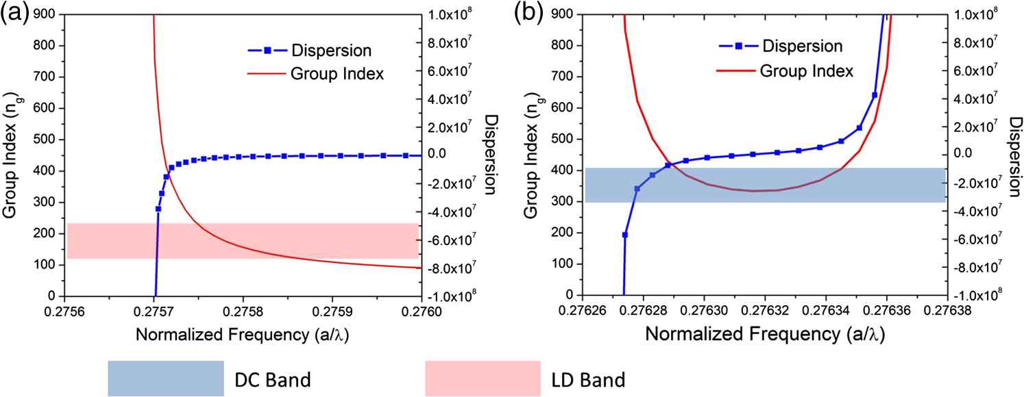 Fig. 4Group index and group-velocity dispersion plot against the normalized frequency of various designs with elliptical hole shift. The line of elliptical holes (a) shifts laterally 150 nm, (b) shifts 160 nm, (c) shifts 170 nm, (d) shifts 180 nm, (e) shifts 190 nm, and (f) shifts half of lattice constant a.  Table 1Summary of group index and bandwidth of various designs of elliptical photonics crystal waveguide.
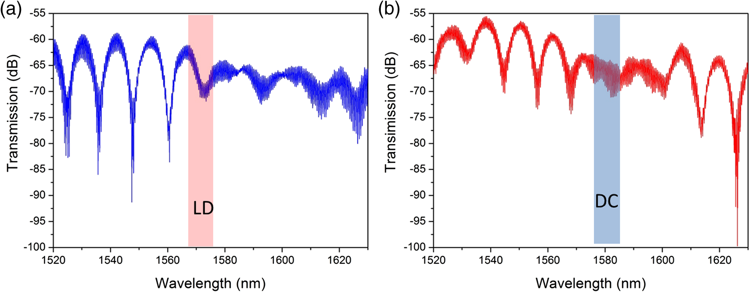
3.Device Fabrication and CharacterizationAs shown in Fig. 5(a), the PhC waveguide embedded in one of the MZI arms with a total length of is fabricated to demonstrate the existence of the slow-light effect. The reference arm is a 440-nm-wide Si strip waveguide. The total length of each arm of the MZI is designed to be between the two Y-shapes beam splitters. The 440-nm-wide Si bus waveguide splits into two beams at the 15-deg Y-shape junction. An optical microscopy image of the fabricated device is shown in Fig. 5(b). The light is coupled in and out from the bus waveguide via two adjacent grating couplers, which are located at the bottom of Fig. 5(b). The spacing between the two grating couplers is , which is designed to fit the fiber array for easy alignment. The entire structure is patterned using electron beam lithography (EBL). Electron beams etch circular and elliptical holes in 200 nm positive resists (ZEP). All the patterns, including the grating couplers, PhC, and waveguides, are predefined in a special format and processed in a single EBL run. Then plasma etching (Deep Reactive Ion Etcher, Oxford 100 Plus) is used to etch away the exposed Si and, hence, transfer the pattern from the resist to the silicon on insulator (SOI) device layer. The fabrication is processed on a 220-nm SOI wafer with a buried oxide layer. Scanning electron microscopy images of the fabricated devices are shown in Fig. 5(c). Figure 5(d) is the magnified image of the fabricated PhC lattice. The lattice constant is designed to be 430 nm in order to center the slow-light region at 1550 nm. Due to the imperfection of the fabrication process, the lattice constant and the radius of the air holes are measured as 439 and 118 nm, respectively. For the ellipse design, the longer and shorter radii are measured as 174 and 75 nm, respectively. The PhC waveguides of a circular lattice are also fabricated as a reference and shown in Figs. 5(e) and 5(f). The radii and the lattice constant are measured as 130 and 441 nm, respectively. Fig. 5(a) Schematic drawing of Mach–Zehnder interferometer (MZI) embedded with PhC waveguide. (b) Optical microscopy image of fabricated MZI device. (c) Scanning electron microscopy (SEM) image of fabricated elliptical PhC waveguide. (d) Zoom-in image of ellipse shape holes. (e) SEM image of fabricated PhC waveguide. (f) Zoom-in image of circular shape holes. 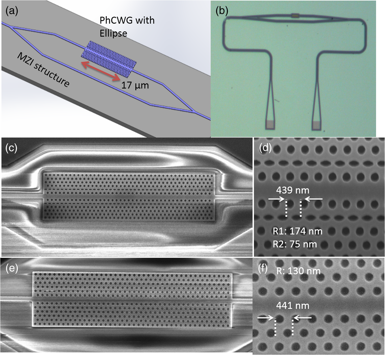 For the testing setups, we use a fiber array attached to a set of six-axis nanostages to achieve ultrafine alignment of the fiber head and grating coupler. The fiber array is made of four polarization maintenance fibers and sealed in a four-in-one V-groove carrier. Two V-grooves are separated by a spacing of and the V-groove carrier is polished to 25 deg together with the fiber heads. The fiber array is aligned vertically above the device surface. The tunable laser source (Agilent 81940A, Santa Clara, California) and optical power sensor (Agilent 81636B) are used for optical signal generation and collection. Figure 6 illustrates the measured spectrum of two designs of the MZI embedded with the PhC slow-light waveguide. The small fluctuation pattern with a 0.5 nm fringe separation shown in the spectrum comes from the Fabry-Perot resonance of the grating coupled backreflections.11 The pass band of the propagation mode of the PhC waveguide as calculated from the band structure plot is indicated in Fig. 6 for both cases of a circular lattice and an elliptical lattice, respectively. They are matched with the measured transmission slow-light interference pattern, which can be read from the plot. The slow-light effect can be observed from the transmission spectrum plot by analyzing the portion with MZI interference. The two designs share the same PhC waveguide effective length as well as the MZI design, and are different in the second line of air holes in PhC waveguides, i.e., data of the elliptical shape shown in Fig. 6(b). From the spectrum plot, we can clearly observe two portions of transmission structure. One is the interference fringes with a free spectrum range of and the other is a relatively flat pattern due to a slow-light interference pattern. However, the slow-light interference pattern of the circular lattice design is much longer than that of the ellipse pattern, since the passing bandwidth of the circular lattice design is much larger than the elliptical lattice design. The slow light interference pattern is relatively larger than the pass band calculated from the band structure. The mismatch of the calculated and the PWE simulated result is due to the imperfection of the fabrication and the finite period of the PhC structure in the real PhC waveguides. The intrinsic losses due to the PhC waveguide also expand and shift the pass band of the fabricated PhC structure. Further optimization of the integrated PhC waveguides and MZI devices will be done to achieve a flat band slow light over a reasonable range, which is desired for various applications. For example, a modulator benefits from its low dispersion and large bandwidth; a delay line benefits from the large group index and small footprint. Moreover, slow-light effect also enhances the study of optical nonlinearities, which can have a great potential in many functions for optoelectronic integrated circuits (OEICs) application. 4.ConclusionIn conclusion, we demonstrated a novel design of dispersion engineered slow-light PhC waveguide. The slow-light performance is optimized by changing the second line of PhC air holes from a circular shape to an elliptical shape. The lateral shift of such a line of elliptical air holes is analyzed through the PWE model approach. The group index and low dispersion bandwidth are optimized to 166 and 1.69 nm, respectively, where the DBP is derived as 0.1812. The optimized PhC using an elliptical lattice design with a lateral shift of 160 nm was fabricated and embedded in an MZI in order to characterize the slow-light characteristics of such an elliptical PhC waveguide. A slow-light interference pattern is observed in both the transmission patterns of MZIs embedded with the ellipse and the circular lattice PhC waveguides. AcknowledgmentsThe authors would like to acknowledge the support by the Academic Research Committee Fund MOE2012-T2-2-154 (Monolithic Integrated Si/AIN Nanophotonics Platform for Optical NEMS and OEICs) and the National University of Singapore under Grant R-263-000-A59-112. ReferencesY. Akahaneet al.,
“Fine-tuned high-Q photonic-crystal nanocavity,”
Opt. Express, 13 1202
(2005). http://dx.doi.org/10.1364/OPEX.13.001202 OPEXFF 1094-4087 Google Scholar
M. LoncarA. SchererY. Qiu,
“Photonic crystal laser sources for chemical detection,”
Appl. Phys. Lett., 82 4648
–4650
(2003). http://dx.doi.org/10.1063/1.1586781 APPLAB 0003-6951 Google Scholar
C. Leeet al.,
“Design and modeling of a nanomechanical sensor using silicon photonic crystals,”
IEEE/OSA J. Lightwave Technol., 26
(7), 839
–846
(2008). http://dx.doi.org/10.1109/JLT.2007.915273 JLTEDG 0733-8724 Google Scholar
B. LiF.-L. HsiaoC. Lee,
“Configuration analysis of sensing element for photonic crystal based NEMS cantilever using dual nano-ring resonator,”
Sens. Actuators A: Phys., 169 352
–361
(2011). http://dx.doi.org/10.1016/j.sna.2011.03.020 SAAPEB 0924-4247 Google Scholar
C. P. Hoet al.,
“Design and modeling of 2-D photonic crystals based hexagonal triple-nano-ring resonators as biosensors,”
Microsyst. Technol., 19
(1), 53
–60
(2013). http://dx.doi.org/10.1007/s00542-012-1610-1 MCTCEF 0946-7076 Google Scholar
S. NodaA. ChutinanM. Imada,
“Tapping and emission of photons by a single defect in a photonic bandgap structure,”
Nature, 407 608
–610
(2000). http://dx.doi.org/10.1038/35036532 NATUAS 0028-0836 Google Scholar
B. S. SongS. NodaT. Asano,
“Photonics devices based on in-plane hetero photonic crystals,”
Science, 300 1537
(2003). http://dx.doi.org/10.1126/science.1083066 SCIEAS 0036-8075 Google Scholar
B. LiF.-L. HsiaoC. Lee,
“Computational characterization of photonic crystal cantilever sensor using hexagonal dual-nano-ring based channel drop filter,”
IEEE Trans. Nanotechnol., 10
(4), 789
–796
(2011). http://dx.doi.org/10.1109/TNANO.2010.2079942 ITNECU 1536-125X Google Scholar
B. LiC. Lee,
“NEMS diaphragm sensors integrated with triple nano ring resonator,”
Sens. Actuators A: Phys., 172
(1), 61
–68
(2011). http://dx.doi.org/10.1016/j.sna.2011.02.028 SAAPEB 0924-4247 Google Scholar
T. Babaet al.,
“50-Gb-s ring-resonator-based silicon modulator,”
Opt. Express, 21 11869
–11876
(2013). http://dx.doi.org/10.1364/OE.21.011869 OPEXFF 1094-4087 Google Scholar
K. Nozakiet al.,
“Ultralow-energy and high-contrast all-optical switch involving Fano resonance based on coupled photonic crystal nanocavities,”
Opt. Express, 21 11877
(2013). http://dx.doi.org/10.1364/OE.21.011877 OPEXFF 1094-4087 Google Scholar
X. Chewet al.,
“An in-plane nano-mechanics approach to achieve reversible resonance control of photonic crystal nanocavities,”
Opt. Express, 18
(21), 22232
–22244
(2010). http://dx.doi.org/10.1364/OE.18.022232 OPEXFF 1094-4087 Google Scholar
F. Tianet al.,
“Tuning of split-ladder cavity by its intrinsic nano-deformation,”
Opt. Express, 20
(25), 27697
–27707
(2012). http://dx.doi.org/10.1364/OE.20.027697 OPEXFF 1094-4087 Google Scholar
T. Baba,
“Slow light in photonics crystal,”
Nat. Photonics, 2 465
–473
(2008). http://dx.doi.org/10.1038/nphoton.2008.146 1749-4885 Google Scholar
M. Shinkawaet al.,
“Nonlinear enhancement in photonic crystal slow light waveguides fabricated using CMOS-compatible process,”
Opt. Express, 19 22208
–22218
(2011). http://dx.doi.org/10.1364/OE.19.022208 OPEXFF 1094-4087 Google Scholar
T. ChenJ. SunL. Li,
“Modal theory of slow light enhanced third-order nonlinear effects in photonic crystal waveguides,”
Opt. Express, 20
(18), 20044
–20058
(2012). http://dx.doi.org/10.1364/OE.20.020043 OPEXFF 1094-4087 Google Scholar
B. Wanget al.,
“Photonic crystal slot nanobeam slow light waveguides for refractive index sensing,”
Appl. Phys. Lett., 97 151105
(2010). http://dx.doi.org/10.1063/1.3497296 APPLAB 0003-6951 Google Scholar
W.-C. Laiet al.,
“Slow light enhanced sensitivity of resonance modes in photonic crystal biosensors,”
Appl. Phys. Lett., 102 041111
(2013). http://dx.doi.org/10.1063/1.4789857 APPLAB 0003-6951 Google Scholar
A. Y. PetrovM. Eich,
“Zero dispersion at small group velocities in photonic crystal waveguides,”
Appl. Phys. Lett., 85 4866
–4868
(2004). http://dx.doi.org/10.1063/1.1815066 APPLAB 0003-6951 Google Scholar
M. D. Settleet al.,
“Flatband slow light in photonic crystals featuring spatial pulse compression and terahertz bandwidth,”
Opt. Express, 15
(1), 219
–226
(2007). http://dx.doi.org/10.1364/OE.15.000219 OPEXFF 1094-4087 Google Scholar
L. H. Frandsenet al.,
“Photonic crystal waveguides with semislow light and tailored dispersion properties,”
Opt. Express, 14
(20), 9444
–9446
(2006). http://dx.doi.org/10.1364/OE.14.009444 OPLEDP 0146-9592 Google Scholar
S. KuBoD. MoriT. Baba,
“Low-group-velocity and low-dispersion slow light in photonic crystal waveguides,”
Opt. Lett., 32 2981
–2983
(2007). http://dx.doi.org/10.1364/OL.32.002981 OPLEDP 0146-9592 Google Scholar
J. Liet al.,
“Systematic design of flat band slow light in photonic crystal waveguides,”
Opt. Express, 16 6227
–6232
(2008). http://dx.doi.org/10.1364/OE.16.006227 OPEXFF 1094-4087 Google Scholar
F. XiaL. SekaricY. Vlasov,
“Ultracompact optical buffers on a silicon chip,”
Nat. Photonics, 1 65
–71
(2007). http://dx.doi.org/10.1038/nphoton.2006.42 1749-4885 Google Scholar
J. B. Khurgin,
“Expanding the bandwidth of slow-light photonics devices based on coupled resonators,”
Opt. Lett., 30 513
–515
(2005). http://dx.doi.org/10.1364/OL.30.000513 OPLEDP 0146-9592 Google Scholar
C. Baoet al.,
“Flat band slow light with high coupling efficiency in one-dimensional grating waveguides,”
IEEE Photonics Technol. Lett., 24
(1), 7
–9
(2012). http://dx.doi.org/10.1109/LPT.2011.2171935 IPTLEL 1041-1135 Google Scholar
J. Houet al.,
“Flat band slow light in symmetric line defect photonic crystal waveguides,”
IEEE Photonics Technol. Lett., 21 1571
–1573
(2009). http://dx.doi.org/10.1109/LPT.2009.2030160 IPTLEL 1041-1135 Google Scholar
C. CaerX. L. RouxE. Cassan,
“Enhanced localization of light in slow wave slot photonic crystal waveguides,”
Opt. Lett., 37 3660
–3662
(2012). http://dx.doi.org/10.1364/OL.37.003660 OPLEDP 0146-9592 Google Scholar
N. JanraoP. ZafarV. Janyani,
“Improved design of photonic crystal waveguides with elliptical holes for enhanced slow light performance,”
Opt. Eng., 51
(6), 064001
(2012). http://dx.doi.org/10.1117/1.OE.51.6.064001 OPEGAR 0091-3286 Google Scholar
A. Casas-Bedoyaet al.,
“Dispersion engineering of wide slot photonic crystal waveguides by Bragg-like corrugation of the slot,”
Opt. Lett., 37 4215
–4217
(2012). http://dx.doi.org/10.1364/OL.37.004215 OPLEDP 0146-9592 Google Scholar
E. Kuramochiet al.,
“Disorder-induced scattering loss of line-defect waveguides in photonic crystal slabs,”
Phys. Rev. B, 72 161318
(2005). http://dx.doi.org/10.1103/PhysRevB.72.161318 PRBMDO 1098-0121 Google Scholar
M. Notomiet al.,
“Extremely large group-velocity dispersion of line-defect waveguides in photonic crystal slabs,”
Phys. Rev. Lett., 87 253902
(2001). http://dx.doi.org/10.1103/PhysRevLett.87.253902 PRLTAO 0031-9007 Google Scholar
S. Rahimiet al.,
“Group-index independent coupling to band engineered SOI photonic crystal waveguide with large slow-down factor,”
Opt. Express, 19 21832
–21841
(2011). http://dx.doi.org/10.1364/OE.19.021832 OPEXFF 1094-4087 Google Scholar
S. G. JohnsonJ. D. Joannopoulos,
“Block-iterative frequency-domain methods for Maxwell’s equations in a planewave basis,”
Opt. Express, 8
(3), 173
–190
(2001). http://dx.doi.org/10.1364/OE.8.000173 OPEXFF 1094-4087 Google Scholar
Y. HamachiS. KuboT. Baba,
“Slow light with low dispersion and nonlinear enhancement in a lattice-shifted photonic crystal waveguide,”
Opt. Lett., 34 1072
–1074
(2009). http://dx.doi.org/10.1364/OL.34.001072 OPLEDP 0146-9592 Google Scholar
BiographyBo Li received his BEng degree and PhD degree from the Department of Electrical and Computer Engineering, National University of Singapore, in 2009 and 2013, respectively. He is currently a research fellow in the same department. His research interests include nanophotonics and its integration with MEMS for sensing applications. Chong Pei Ho received his BEng degree from Department of Electrical and Computer Engineering at National University of Singapore in 2011. He is currently a research engineer in the same department and has been enrolled in the NUS PhD program since January 2012. His research interests include applications involving nanophotonics. Fu-Li Hsiao received his BS degree from the Department of Physics of National Changhua University of Education, Taiwan, in 2002 and his PhD degree in FEMTO-ST from the University of Franche-Comte, France, and from the Department of Optics and Photonics of National Central University, Taiwan, in 2008. He has been a postdoctoral research fellow in the Department of Electrical and Computer Engineering at National University of Singapore from 2008 to 2009. Currently, he is an associate professor in the Institute of Photonics at National Changhua University of Education, Changhua City, Taiwan. His research interests include photonic crystals, phononic crystals, and optical MEMS. Chengkuo Lee received his MS degree in materials science and engineering from National Tsing Hua University, Hsinchu, Taiwan, in 1991. He also received his MS degree in industrial and system engineering from Rutgers University, New Brunswick, New Jersey, USA, in 1993. He received his PhD degree in precision engineering from the University of Tokyo, Tokyo, Japan, in January 1996. From 2006 to 2009, he was a senior member of technical staff at the Institute of Microelectronics, A*Star, Singapore. Currently, he is an associate professor at the Department of Electrical and Computer Engineering of National University of Singapore, Singapore. |