|
|
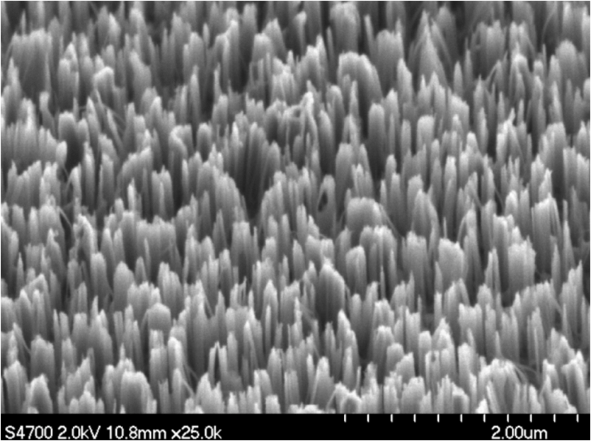
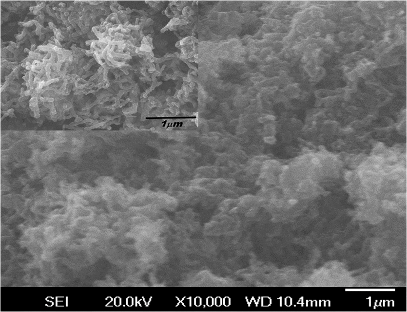
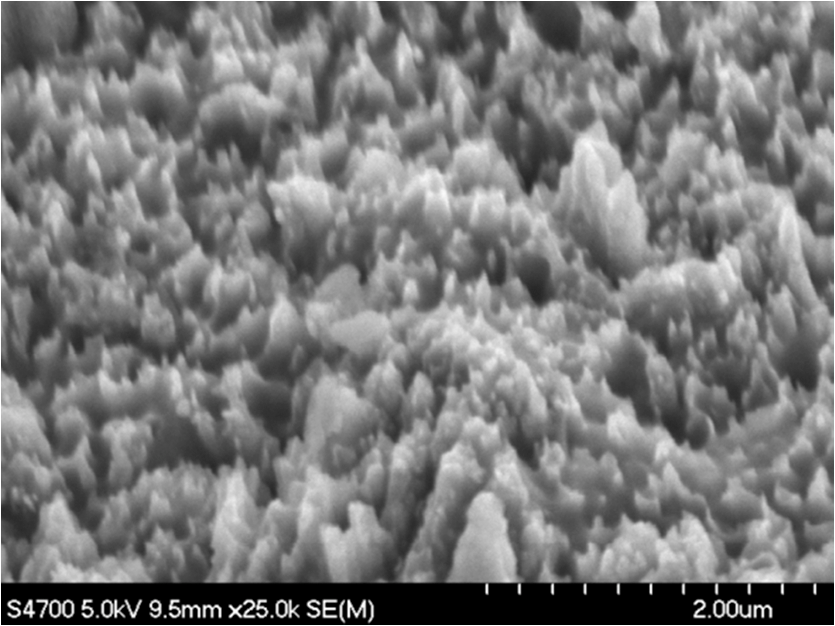
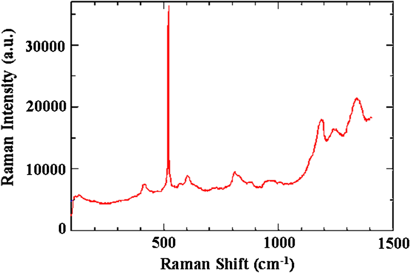
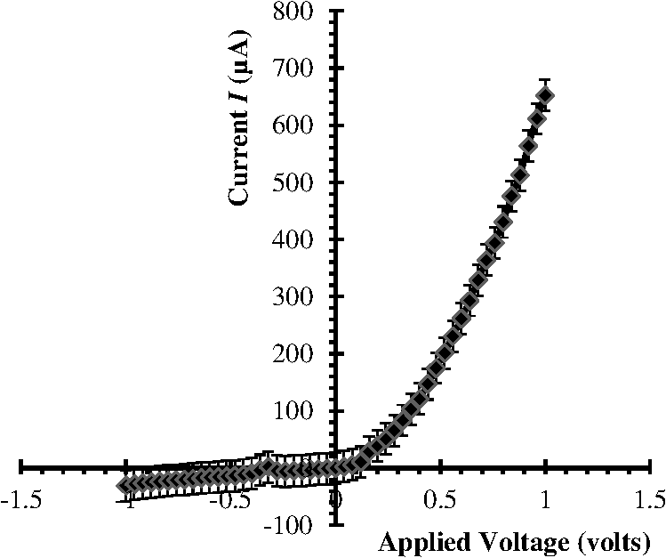
1.IntroductionThe intense attention and research on conducting polymers have led to a number of practical applications because of their unique electronic properties, diversity, ease of fabrication and potentially low cost. Intrinsically conducting polymers, including polyacetylene, polyaniline (PANI), polypyrrole, polythiophene, poly(p-phenylene-vinylene), etc., are termed organic polymers that possess the electrical, magnetic, and optical properties of a metal while retaining the mechanical property and processability commonly associated with a conventional polymer. These polymers are more commonly known as “synthetic metals.”1,2 Since most organic polymers do not have intrinsic charge carriers, the required charge carriers may be provided by partial oxidation (-type redox doping) of the polymer chain with electron acceptors, or by partial reduction (-type redox doping) with electron donors. Through such a doping process, charged defects (e.g., polaron, bipolaron, and soliton) are introduced, which could then be available as the charge carriers enabling conjugated polymers to gain high conductivities. Conducting polymers are sometimes considered as quasi-one dimensional metals due to the fact that the strong interchain interactions (strong covalent bonding along the chain), and the weak Van der Waals type interchain coupling interactions lead to the delocalization of -electrons along the polymer chain. Every conjugated polymer has a unique chemical structure that determines its optical and electrical behavior. PANI and its derivatives have attracted significant interest as electronic materials because of their high capacity, good conductivity, unique doping and de-doping processes, and ease of synthesis.3 Poly (o-toluidine) (POT) is a PANI derivative which contains a methyl group in the ortho position of the aniline monomer. Among the ring-substituted PANI derivatives, POT has probably been the most widely studied.4 Indeed, Ram and Borol as well as other authors had studied the electro polymerization of POT using various electrolytes with different concentrations. Research revealed that POTs have interesting electro-optical properties and can be used as electrochromic and electronic devices.5–7 Recently, conductive polymer nanostructures have attracted a great deal of interest for use in energy applications because of several beneficial characteristics including tunable electrical properties, flexibility, and their processability, mainly by dispersion.8,9 Recently, the interest in nanostructured PANI, especially, PANI nanofibers, has increased extensively.3,10 On the other hand, porous silicon (PSi) nanostructures were found to be perfect to host the polymerization of conducting polymers to form a conducting polymer/PSi heterojunction.11 Heterojunction devices have also drawn great attention in recent years mainly due to their use in optoelectronic fields. The properties of those heterojunctions are important as they are used as field-effect transistors (FETs), bipolar transistors, light emitting diodes, and lasers. The heterojunction diode could present a great potential for its use in sensing applications.4,12 Numerous synthesis techniques have been currently developed for various types of nanomaterials. However, there is a large area to be improved, which is the preparation of large-area uniform nanostructure arrays, especially through controllable, facile approaches. SiNWs are expected to work as building blocks and interconnect nanoscale electronic and optoelectronic devices. SiNWs-based nanodevices such as biological sensors, FETs, and integrated logic circuits have been demonstrated as powerful examples in applications. Currently, different methods have been utilized to fabricate SiNWs.13–16 Compared with PSi heterojunctions, the aligned one-dimensional (1-D) SiNWs arrays offer a promising substrate which can provide a direct pathway of charge transport and high mobility for carriers.17 Thus, SiNWs are expected to play an important role in enhancement of the characteristics of the fabricated heterojunction diodes. In the present paper, the use of a thin film of the conducting polymer “POT” replacing the metal in a Schottky barrier diode forms a new heterojunction diode with nearly similar characteristics. The conducting polymer may be preferable because electronic devices based on conjugated polymers can be more easily processed at low temperatures using inexpensive technologies. In the present work, an NPOT/SiNWs heterojunction is proposed to be a good candidate for heterojunction diode with enhanced electrical properties. A technique to fabricate a high quality NPOT/SiNWs heterojunction diode is described. Good reproducibility of the electrical characteristics is reported. It is worth mentioning that these characteristics are required for possible sensing applications. 2.Experimental ProceduresSiNWs have been fabricated using an improved metal-assisted electroless etching of Si substrates in solution. A p-type Si (100) wafer with a resistivity around 1 Ωcm has been used. The wafer has been cut into pieces to be used as test samples. Si samples have been ultrasonically cleaned in acetone, absolute alcohol, and deionized water successively. Then the cleaned Si samples have been dipped into dilute HF solution to remove any native oxide. After this cleaning step, an etching process has been performed by immersing Si samples into the etching solution, which contains 5 M HF, 0.02 M , and 0.05 M . The reaction has been left for 15 min. Then the Si samples have been rinsed with deionized water and immersed into the concentrated to remove the remaining silver and other residues. The NPOT films have been chemically fabricated via in situ polymerization. The use of an in situ polymerization method has been preferred because the spin coating approach would be difficult to implement since very few solvents are available for the dissolution of PANI or POT for subsequent spin coating. In addition, spin-coated conducting polymer films frequently suffer from poor adhesion to the surface of the support layer. On the other hand, in situ deposition polymerization of POT is a simple, continuous, and scalable method for the production of smooth thin films.18 In the case of silicon micro or nanostructures, the in-situ polymerizations are expected to provide a better coverage than the spin coating method. Thus, in-situ polymerization finally enhances the quality of the thin film of the conducting polymer. Ammonium persulfate (APS) has been used as the oxidant of the polymerization process. Purified o-toluidine (OT) (0.05 M) has been dissolved in 50 ml of 0.03 M sodium dodecyl sulfate (SDS) solution. HCl (50 ml of 0.1 M) aqueous solution which contains 0.05 M of APS has been added into the previous OT solution under stirring. Five ml of this mixture has been added to the silicon surface and has been left for 1 h at room temperature. The molar ratio of APS as an oxidant to OT is . During the polymerization of OT, the originally colorless mixture turns blue and later becomes dark green. The dark green color is an indication of the formation of the required salt formation. The Si wafer has been washed with 0.1 M HCl solution and then dried at 60°C for 24 h in a vacuum desiccator. The precipitate has been collected and washed with methanol to remove the unreacted monomer and the impurities followed by a 0.1 M HCl aqueous solution wash. The precipitate has been dried at 60°C for 24 h in a vacuum desiccator. An ohmic contact has been made on the bottom of the heterojunction using aluminum (Al) evaporation under vacuum. The other ohmic contact has been made by thermal evaporation under vacuum of 50 nm of gold (Au) onto the conducting polymer. 3.Results and Discussion3.1.Mechanism of the Formation of SiNWs ArrayEtching of Si with HF solution (5 M HF, 0.05 M , and 0.02 M ) to produce vertical SiNWs includes two main reactions as shown below: The initial reduction of forms Ag nanoparticles on the Si wafer surface. A vertical alignment contributes to the longitudinal falling down of the Ag nanoparticles from the surface to the bulk of the Si substrates, along with continuous dissolution of Si in the vicinity of Ag particles.19,20 Figure 1 shows a planar top view of an SEM image (at a 45 deg tilt angle). It shows the micrograph of the prepared SiNWs array. The morphology of SiNWs indicates that they are uniform on the entire wafer surface with diameters in the range of 50 to 200 nm. Also, they are vertical to the wafer surface. 3.2.Characterization of NPOT3.2.1.FTIR spectroscopy of POTUV−vis spectra indicate that POT exists as a conductive emeraldine salt as shown in Fig. 2(a). It is noticed that there are two peaks near 360 and 698 nm as well as a long absorption band. The 360 nm peak is attributed to the transition of POT’s benzenoid ring. The peak at 698 nm and the long absorption band is attributed to polaron bands, which are characteristic of a conductive emeraldine salt. FTIR spectra of the polymer materials (in KBr pellets) were recorded on JASCO FTIR 410 spectrophotometer. Figure 2(b) represents the IR spectrum for doped NPOT. Fig. 2(a) UV-visible spectrum of the synthesized NPOT film deposited on a glass substrate. (b) FTIR spectrum of the fabricated NPOT film. 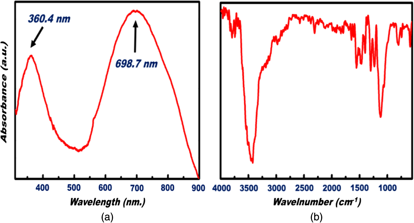 The main characteristic bands of doped PANI are assigned as follows: the characteristic sharp band at 1220 to is due to C–N tertiary aromatic vibration, the bands at 1360, 1250, 1340 and are due to C–N primary and secondary vibrations. The sharp characteristic band at the range 3450 to is due to single bridge compounds polymeric association or to NH stretching vibration. The bands at 1550 and are due to the presence of a quinoid structure and the band at is due to C–N stretching mode for the benzenoid ring. The band at is characteristic of a para-substituted aromatic ring, and it reveals that polymerization has proceeded in a “head to tail” form. Both UV–vis and FTIR results reveal that the POT nanostructure is that of a typical doped polymer in its emeraldine salt form.21,22 3.2.2.X-ray of NPOTFigure 3 shows the X-ray diffraction (XRD) patterns of NPOT, and the X-ray profile shows three well-defined peaks for the POT prepared. The peaks are observed at , 20 deg, and 25 deg. The maximum peak at around 25 deg can be assigned to the scattering from the POT chains at the interplanar spacing. On the other hand, two broad peaks centered at and 20 deg may be ascribed to the periodicity parallel to the polymer chains, while the latter peaks may be caused by the periodicity perpendicular to the polymer chains.23 The XRD patterns may, therefore, suggest that the obtained nanostructured POT has some crystallinity.24 3.2.3.SEM characterization of NPOTA scanning electron microscope (SEM) has been used to investigate the surface morphology of the synthesized NPOT. In the SEM micrographs as in (Fig. 4), rod-like shape nanostructures can be distinguished. 3.3.Characterization of NPOT/Si NWs HeterojunctionFigure 5 shows the SEM micrograph after the deposition of the chemically synthesized NPOT upon the fabricated SiNWs. The deposition of NPOT has been found to be homogenous upon the fabricated SiNWs. Figure 6 shows the resonance Raman spectra of POT nanofibers after the deposition on silicon nanowires. These spectra have been obtained by using a Raman mapping laser of wavelength 532 nm in room temperature under atmospheric pressure. The Si signal is a single peak, as is well-known, at . The other peaks of POT are also in good agreement with values published in literature.25 3.4.characteristics of the Synthesized HeterojunctionThe characteristics of the heterojunction diode Au/NPOT/SiNWs/Al is shown in Fig. 7. According to the curve shown in Fig. 7, it is noticed that the curve possesses good diode characteristics which clearly demonstrates the occurrence of a rectifying junction. The curve shows that the turn-on voltage is about 0.2 V, which is much lower than the Si p-n diode (0.6 to 0.7 V) and is similar to a Schottcky diode (0.2 to 0.3 V). The low forward voltage drop allows a lower power loss than ordinary Si p-n junction diodes. Therefore, it may be suggested that this fabricated NPOT/SiNWs heterojunction diode can be used as a Schottky diode in ultrafast switches in electronic circuits.26–28 With an assumption that the current is due to thermionic emission, the current in the device can be analyzed by using thermionic emission theory. According to this theory, the relation between the current and voltage of the device can be expressed as29 where is the reverse saturation current and is expressed as follows: where is the electron charge, is the applied voltage, is the effective Richardson constant equal to for p-type,30,31 is the effective diode area, is the absolute temperature, is the Boltzmann constant, is the ideality factor, and is the barrier height. The value of can be determined from the slope of the linear region of the forward bias semi log characteristics through the equation 30,32The barrier height can be obtained from the following equation:33 Since the current curve in forward bias quickly becomes dominated by series resistance and deviates from linearity, so the low forward bias part of the characteristics should be used to calculate the ideality factor. The ideality factor can be calculated according to the natural logarithm () plot according to the following equation: According to Eq. (5) the () plot is shown in Fig. 8. From Fig. 8 and by using Eq. (5), and can be calculated from the slope and the -axis intercept of the fitted straight line, respectively. and are found to be 1.8 and A. From Eq. (4), the barrier height can also be calculated and it is found to be 0.74 eV. It had been reported in literature that the previous method of calculating may be not very accurate. The reason this may be that this method only works for diodes with low series resistance which can be neglected in the low forward region of the curve. This may not be satisfied in many heterojunctions.33 Therefore, in the present work, other methods of calculations have been taken into consideration to confirm the value of and also to confirm the values of other parameters of the fabricated heterojunction. The Cheung method is a second and efficient method to calculate and to confirm the values of and calculated with the above method. The Cheung method had been found to be helpful and convenient to check the validity of the diode-series resistor model because deviations from straight lines can easily be detected.34 The forward bias current–voltage characteristics due to thermionic emission of a Schottky barrier diode with series resistance can be expressed as a Cheung function given by the following equations: The experimental versus plot of our heterojunction diode at the temperature of 293 K is presented in Fig. 9. Fig. 9versus plot of NPOT/SiNWs heterojunction diode at the temperature of 293 K in dark conditions.  By taking the trend straight line of the curve and using Eq. (7), and can be determined from the intercept and the slope of the line, respectively. and were determined as 1.7 KΩ and 1.9565, respectively. It can be seen that the value of obtained by this method is in agreement with the value determined by applying the thermionic emission theory to the characteristics. Using the value determined from Eq. (8), a plot of versus as shown in Fig. 10 gives a straight line with a -axis intercept that is equal to and a slope that provides a second determination of . In this method, the least square fitting approach has been used which gives us the opportunity of using more data points and hence increasing the accuracy of our calculations. From Fig. 10 and by using Eq. (8), the values of and are determined as 0.844 eV and 1.4 KΩ, respectively. Therefore, using Cheung’s approach has provided a second determination of which is approximately close to the value derived from the previous method of calculations. and values of the fabricated NPOT/SiNWs heterojunction have been found to be lower than and values previously published for a NPANI/PSi heterojunction.35–39 In the present work, the of the fabricated NPOT/SiNWs has become lower than the published values. This finding may be explained as being due to the use of SiNWs, providing a 1-D nanowire array which offers a promising substrate with a direct pathway for charge transport and a high mobility for carriers.17 Regardless of these details, the low and values obtained in the present work are promising for the fabrication of high quality NPOT/SiNWs heterojunctions. El-Menyawy and Ashery had reported current–voltage characteristics of Au/poly(o-toluidine)/p-Si/Al heterojunction diode, where a thin film of POT had been prepared onto the surface of p-Si single crystal by a spin coating technique. They found a value for the barrier height which is in good agreement with ours. As for the ideality factor, they had reported that the ideality factor values extracted from the natural logarithm () plot and from the versus plot were 2.63 and 4.06, respectively. In our case, the ideality factor values have been found 1.8 and 1.9565, which are lower than El-Menyawy’s group values.40 The exact mechanism of a high ideality factor has not been fully understood yet. However, in literature, some researchers had reported that a higher value of suggests that the carrier recombination in the Si substrate may be significant in the conduction mechanism.34 Some others had suggested that the ideality factor is high due to the use of PSi as a substrate, therefore, at the interface of the heterojunction, the defect density is very high.37 It is worth mentioning that El-Menyawy and Ashery had reported that the series resistance values extracted from the versus plot and Cheung plot had been found to be 494 and 446 Ω, respectively which, are lower than the 1700 and 1400 Ω series resistance values found by our group. Their lower values than ours may be due to the high voltage region in which their calculations had been made by using the Cheung method. Also, it may be due to any other conditions during their fabrication process. 4.ConclusionsA high quality NPOT/SiNWs heterojunction has been fabricated by using low cost and simple techniques, where the SiNWs have been fabricated by using improved metal-assisted electroless chemical etching of silicon in solution. The device presents reproducibility of electrical characteristics and a good rectifying behavior. The saturation current has been found to be A. The barrier height has been at about 0.79 eV. The ideality factor has been found to be close to 2. The series resistance has been found to be about 1.55 KΩ. A low turn-on voltage (0.2 V) associated with the fabricated heterojunction may give the possibility of being used in ultrafast switching and other useful applications. The series resistance has been found to have a lower value than the values reported for similar PSi heterojunctions. Enhancement of the proposed heterojunction parameters is suggested to be related to the unique properties of SiNWs compared to PSi and may also be related to the use of in situ polymerization rather than spin coating because in situ polymerization can offer good coverage of the surface and sufficient polymerization of NPOT on SiNWs. AcknowledgmentsI am heartily thankful to Prof. Masaya Ichimura, as we confirmed the I-V characteristics in his laboratory, Nagoya Institute of Technology, Nagoya, Japan. I am also grateful to Prof. Samia Saafan, professor of physics at Tanta University, for her guidance and support to revise the manuscript. ReferencesP. PalK. Sato,
“Fabrication methods based on wet etching process for the realization of silicon MEMS structures with new shapes,”
Microsyst. Technol., 16
(7), 1165
–1174
(2010). http://dx.doi.org/10.1007/s00542-009-0956-5 0946-7076 Google Scholar
A. G. MacDiarmid,
“Synthetic metals: a novel role for organic polymers,”
Synth. Met., 125
(1), 11
–22
(2001). http://dx.doi.org/10.1016/S0379-6779(01)00508-2 SYMEDZ 0379-6779 Google Scholar
J. Liet al.,
“A gas sensor array using carbon nanotube and microfabrication technology,”
Electrochem. Solid State Lett., 8
(11), 100
–102
(2005). http://dx.doi.org/10.1149/1.2063289 ESLEF6 1099-0062 Google Scholar
K. M. Zaidanet al.,
“Synthesis and characterization of poly (o-toluidine) POT blend with polyethylene oxide PEO as conducting polymer alloys,”
Der Chem. Sin., 3
(4), 841
–848
(2012). Google Scholar
S. Choet al.,
“Enhanced electrochemical performance of highly porous supercapacitor electrodes based on solution processed polyaniline thin films,”
ACS Appl. Mater. Interfaces, 5
(18), 9186
–9193
(2013). http://dx.doi.org/10.1021/am402702y AAMICK 1944-8244 Google Scholar
M. K. Ramet al.,
“Electrochemical and optical characteristics of conducting poly(o-toluidine) films,”
Thin Solid Films, 304
(1–2), 65
–69
(1997). http://dx.doi.org/10.1016/S0040-6090(97)00186-7 THSFAP 0040-6090 Google Scholar
D. D. Boroleet al.,
“Effect of inorganic dopants (in presence of electrolyte) on the conductivity of polyaniline, poly(o-toluidine) and their copolymer thin films,”
Mater. Lett., 57
(4), 844
–852
(2002). http://dx.doi.org/10.1016/S0167-577X(02)00883-2 MLETDJ 0167-577X Google Scholar
N. Tuglugluet al.,
“Temperature dependence of current–voltage characteristics of Ag/p-SnSe Schottky diodes,”
Appl. Surf. Sci., 233
(1–4), 320
–327
(2004). http://dx.doi.org/10.1016/j.apsusc.2004.03.238 ASUSEE 0169-4332 Google Scholar
Y. XiaK. SunJ. Ouyang,
“Solution-processed metallic conducting polymer films as transparent electrode of optoelectronic devices,”
Adv. Mater., 24
(18), 2436
–2440
(2012). http://dx.doi.org/10.1002/adma.201104795 ADVMEW 0935-9648 Google Scholar
G. Marjanović,
“Polyaniline nanostructures,”
Nanostructured Conductive Polymers, 19
–98 John Wiley & Sons Ltd., Chichester, United Kingdom
(2010). Google Scholar
P. GranitzerK. Rumpf,
“Porous silicon–a versatile host material,”
Materials, 3
(2), 943
–998
(2010). http://dx.doi.org/10.3390/ma3020943 MATEG9 1996-1944 Google Scholar
J. M. G. Laranjeiraet al.,
“Conducting polymer/silicon heterojunction diode for gamma radiation detection,”
Radiat. Prot. Dosim., 101
(1–4), 85
–88
(2002). Google Scholar
M. L. Zhanget al.,
“Preparation of large-area uniform silicon nanowires arrays through metal-assisted chemical etching,”
J. Phys. Chem. C, 112
(12), 4444
–4450
(2008). http://dx.doi.org/10.1021/jp077053o 1932-7447 Google Scholar
Z. Li,
“Sequence-specific label-free DNA sensors based on silicon nanowires,”
Nano Lett., 4
(2), 245
–247
(2004). http://dx.doi.org/10.1021/nl034958e NALEFD 1530-6984 Google Scholar
J. HahmC. M. Lieber,
“Direct ultrasensitive electrical detection of DNA and DNA sequence variations using nanowire nanosensors,”
Nano Lett., 4
(1), 51
–54
(2004). http://dx.doi.org/10.1021/nl034853b NALEFD 1530-6984 Google Scholar
Y. Cui,
“Nanowire nanosensors for highly sensitive and selective detection of biological and chemical species,”
Science, 293
(5533), 1289
–1292
(2001). http://dx.doi.org/10.1126/science.1062711 SCIEAS 0036-8075 Google Scholar
J. M. G. Laranjeiraet al.,
“Fabrication of high quality silicon–polyaniline heterojunctions,”
Appl. Surf. Sci., 190
(1–4), 390
–394
(2002). http://dx.doi.org/10.1016/S0169-4332(01)00901-1 ASUSEE 0169-4332 Google Scholar
N. V. Blinovaet al.,
“Effect of reaction conditions on film morphology of polyaniline composite membranes for gas separation,”
J. Polym. Sci. A, 50
(15), 3077
–3085
(2012). http://dx.doi.org/10.1002/pola.26093 JPACEC 0887-624X Google Scholar
V. Sivakovet al.,
“Wet—chemically etched silicon nanowire architectures: formation and properties,”
Nanowires Fundmental Research, InTech, Croatia
(2011). http://dx.doi.org/10.5772/16736 Google Scholar
Z. Huanget al.,
“Metal-assisted chemical etching of silicon: a review,”
Adv. Mater., 23
(2), 285
–308
(2011). http://dx.doi.org/10.1002/adma.v23.2 ADVMEW 0935-9648 Google Scholar
T. AbdiryimZ. GangR. Jamal,
“Synthesis and characterization of poly(o-toluidine) doped with organic sulfonic acid by solid-state polymerization,”
J. Appl. Polym. Sci., 96
(5), 1630
–1634
(2005). http://dx.doi.org/10.1002/(ISSN)1097-4628 JAPNAB 1097-4628 Google Scholar
Z. MucukM. KarakislaM. Sacak,
“Synthesis of poly(o-toluidine) in DMF/ water mixture using benzoyl peroxide,”
Int. J. Polym. Anal. Charact., 14
(5), 403
–417
(2009). http://dx.doi.org/10.1080/10236660903031025 IPACEZ 1023-666X Google Scholar
R. Douaniet al.,
“Silver-assisted electroless etching mechanism of silicon,”
Phys. Stat. Sol., 205
(2), 225
–230
(2008). http://dx.doi.org/10.1002/pssa.v205:2 PHSSAK 0031-8957 Google Scholar
W. Feng,
“Synthesis and characterization of photoconducting polyaniline-TiO2 nanocomposite,”
Bull. Chem. Soc. Japan, 73
(11), 2627
–2633
(2000). http://dx.doi.org/10.1246/bcsj.73.2627 BCSJA8 0009-2673 Google Scholar
G. Ćirić-MarjanovićM. TrchováJ. Stejskal,
“The chemical oxidative polymerization of aniline in water: Raman spectroscopy,”
J. Raman Spectrosc., 39
(10), 1375
–1387
(2008). http://dx.doi.org/10.1002/jrs.v39:10 JRSPAF 0377-0486 Google Scholar
K. Hess, Advanced Theory of Semiconductor Devices, 2nd ed.IEEE Press, New York
(2000). Google Scholar
T. Jeevanandaet al.,
“Preparation of polyaniline nanostructures using sodium dodecylsulphate,”
Mater. Lett., 62
(24), 3995
–3998
(2008). http://dx.doi.org/10.1016/j.matlet.2008.05.041 MLETDJ 0167-577X Google Scholar
L. Brillson, Contacts to Semiconductors, Fundamentals and Technology, Noyes Press, Park Ridge, NJ
(1993). Google Scholar
C. A. Betty,
“Highly sensitive capacitive immunosensor based on porous silicon–polyaniline structure: Bias dependence on specificity,”
Biosens. Bioelectron., 25
(2), 338
–343
(2009). http://dx.doi.org/10.1016/j.bios.2009.07.009 BBIOE4 0956-5663 Google Scholar
Z. Zhanget al.,
“Highly crystalline and thin polyaniline nanofibers oxidized by ferric chloride,”
Mater. Chem. Phys., 115
(1), 275
–279
(2009). http://dx.doi.org/10.1016/j.matchemphys.2008.12.005 MCHPDR 0254-0584 Google Scholar
M. PattabiS. KrishnanX. Mathew,
“Effect of temperature and electron irradiation on the I–V characteristics of Au/CdTe schottky diodes,”
Sol. Energy, 81
(1), 111
–116
(2007). http://dx.doi.org/10.1016/j.solener.2006.06.004 SRENA4 0038-092X Google Scholar
T. Hoshiet al.,
“Low-turn-on-voltage heterojunction bipolar transistors with a C-doped InGaAsSb base grown by metalorganic chemical vapor deposition,”
Jpn. J. Appl. Phys, 51 04DF01
(2012). http://dx.doi.org/10.7567/JJAP.51.04DF01 JJAPA5 0021-4922 Google Scholar
M. A. YeganehS. H. Rahmatollahpur,
“Barrier height and ideality factor dependency on identically produced small Au/p-Si Schottky barrier diodes,”
J. Semicond., 31
(7), 074001
(2010). http://dx.doi.org/10.1088/1674-4926/31/7/074001 JSOEB4 1674-4926 Google Scholar
Z.-F. Caoet al.,
“Determination of the series resistance under the Schottky contacts of AlGaN/AlN/GaN Schottky barrier diodes,”
Chin. Phys. B, 21
(1), 0171031
(2012). http://dx.doi.org/10.1088/1674-1056/21/1/017103 1674-1056 Google Scholar
S. K. CheungN. W. Cheung,
“Extraction of Schottky diode parameters from forward current-voltage characteristics,”
Appl. Phys. Lett., 49
(2), 85
–87
(1986). http://dx.doi.org/10.1063/1.97359 APPLAB 0003-6951 Google Scholar
S. El-Zoharyet al.,
“Electrical characterization of nanopolyaniline/porous silicon heterojunction at high temperatures,”
J. Nanomater., 2013
(2013), 1
–8
(2013). http://dx.doi.org/10.1155/2013/568175 1932-7447 Google Scholar
A. Asheryet al.,
“Fabrication and characterization of in situ polymerized n-polyaniline films grown on p-Si heterojunctions,”
Microelectron. Eng., 85 2309
–2315
(2008). http://dx.doi.org/10.1016/j.mee.2008.08.003 MIENEF 0167-9317 Google Scholar
P. Kumaret al.,
“Fabrication and characterization of polyaniline/porous silicon heterojunction,”
Synth. Met., 160
(13–14), 1507
–1512
(2010). http://dx.doi.org/10.1016/j.synthmet.2010.05.011 SYMEDZ 0379-6779 Google Scholar
R. PoddarC. Luo,
“A novel approach to fabricate a PPy/p-type Si heterojunction,”
Solid-State Electron., 50
(11–12), 1687
–1691
(2006). http://dx.doi.org/10.1016/j.sse.2006.10.006 SSELA5 0038-1101 Google Scholar
E. El-MenyawyA. Ashery,
“Current–voltage characteristics and inhomogeneous barrier height analysis of Au/poly(o-toluidine)/p-Si/Al heterojunction diode,”
J. Mater. Sci., 25
(9), 3939
–3946
(2014). http://dx.doi.org/10.1007/s10854-014-2110-0 JMTSAS 0022-2461 Google Scholar
BiographySalah E. El-Zohary received his BS degree from the Physics Department, Faculty of Science, Tanta University, Egypt, in 2004, where he was appointed as a demonstrator. He received his MS degree in 2011 and his PhD degree in 2014, from the Department of Optical System Engineering, University of Tokushima, Japan. He was appointed as assistant lecturer in 2011 and as a lecturer in 2014 in the Physics Department, Faculty of Science, Tanta University. His primary research focuses on novel nanofabrications for advanced nanophotonic and optoelectronic devices. Mohamed A. Shenashen received his PhD in 2008. He joined the Optical Science and Technology Department, Tokushima University, Japan, as a postdoctoral researcher for 2 years. He was awarded an NIMS postdoctoral research fellowship in the group of Professor Sherif A. El-Safty to work on the design of nanomaterials for a wide range of daily and environmental applications such as energy and environmental pollutants recovery since in 2010. He is also a researcher in Petrochemical Department, Egyptian Petroleum Research Institute (EPRI), Cairo, Egypt. Ashraf M. Abdel Haleem received his BS degree in electronics and electrical communications from Cairo University (Egypt) in 1998. He received his MS degree in engineering physics from Cairo University in 2003. He received his PhD degree from Nagoya Institute of Technology (Japan) in 2010. He has been engaged in research on semiconductor thin film deposition, characterization, and application for solar cells and artificial artificial photosynthesis. Akinori Tsuji received his BE degree from the University of Tottori in 1998. He received his ME and PhD degrees from the University of Tokushima in 2002 and 2013, respectively. He has been an engineer in the Department of Information Science and Intelligent Systems at the University of Tokushima since 1998. His research interests include image and digital signal processing, nonlinear circuit analysis, and embedded systems. Toshihiro Okamoto received his MEng in electric and electronic engineering from the University of Tokushima, Japan, in 1993 and his PhD in engineering from the University of Tokushima in 2000. Since 2014, he has been an associate professor at the University of Tokushima. His primary research areas are nonlinear photonics of surface plasmons and metamaterials. Masanobu Haraguchi received his PhD degree from Osaka University in 1993. Since 2009, he has been a professor at the University of Tokushima. He is interested in characteristics and applications of localized and propagating plasmons at nanometal structure. Recently, his main interests are active devices using channel type plasmonic waveguides and applications of split ring resonators for NIR and visible region. |