|
|
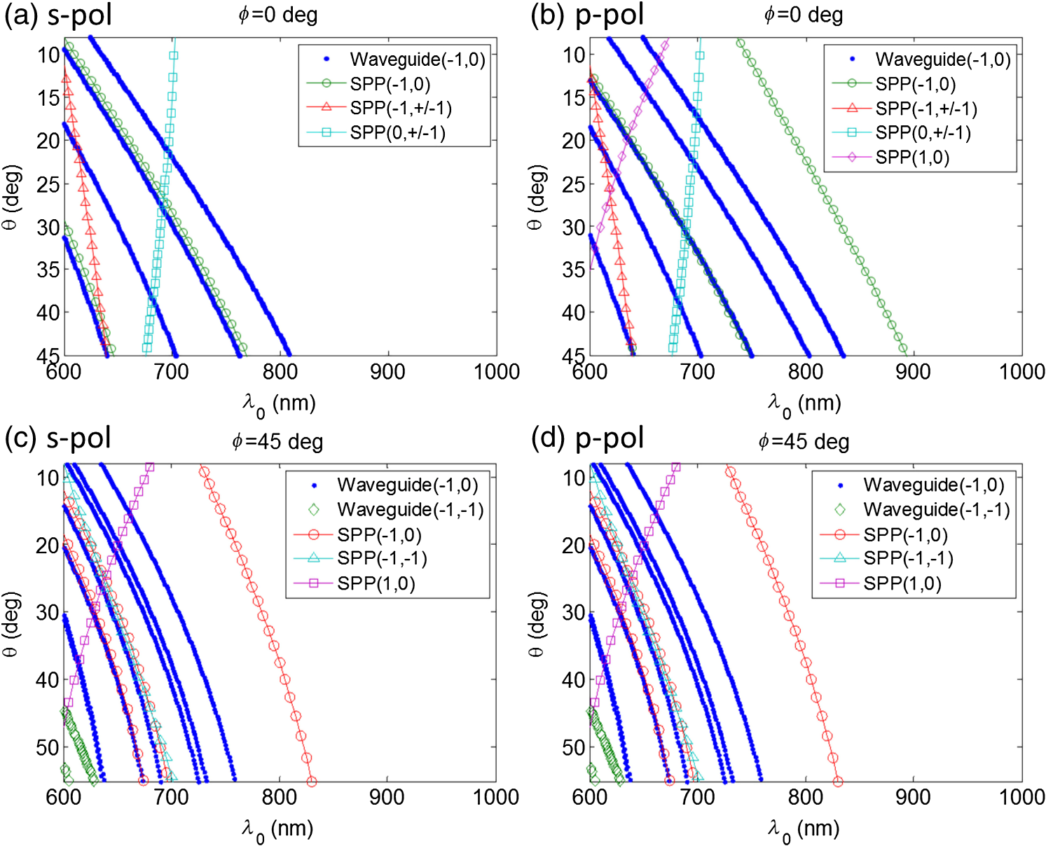
1.IntroductionSurface-plasmon-polariton (SPP) waves are electromagnetic surface waves guided by the planar interface of a dielectric material and a metal.1 These waves are commonly exploited for optical sensing2 and biosensing,3 optical filtering,4 and photo detection.5 Of particular interest, in recent years, has been their application for photovoltaic6 and photoelectrochemical7 energy-harvesting devices, because their excitation can offer light-absorption enhancement exceeding the Lambertian limit.8 Although absorption enhancement by SPP waves in photovoltaic devices has been studied for more than three decades,9–12 significant improvements in device performance have not been reported yet. This is because the SPP waves can only enhance the absorption by a small amount—since (1) only incident -polarized light (magnetic field perpendicular to the incidence plane) can excite SPP waves and (2) only one SPP wave can be excited at a specific free-space wavelength when the dielectric material is homogeneously normal to the interface.13 In addition, the field is confined in a subwavelength region near the interface, leading to high absorption in the metal and limited enhancement in the active device region that is usually quite far from the interface.12 When the dielectric material is of finite thickness, the air/dielectric/metal structure can act as an open-face slab waveguide.14,15 The fields of the waveguide modes are largely confined to the dielectric slab and depend on the thickness of that slab. These waveguide modes can also enhance the electric field and, therefore, the electron–hole pair generation rate, in photovoltaic solar cells.16–18 When the dielectric material is periodically nonhomogeneous in the thickness direction, multiple SPP waves can be guided by its interface with the metal.13,19 The excitation of the multiple SPP waves has been experimentally confirmed 20–22 over a broad range of incidence angles and wavelengths. Furthermore, the underlying surface-multiplasmonics theory19 shows that light absorption in thin-film solar cells can be increased by introducing periodic nonhomogeneity in the semiconductor material.23 Finally, because the propagation length of some of the multiple SPP waves in this structure is predicted to be as long as millimeters, the interface can be potentially exploited as a planar solar concentrator.24 Most often, experimental excitation of SPP waves requires either the use of a coupling prism or the periodic corrugation of the metal/dielectric interface.25 For a solar-energy-harvesting application, the use of a prism9 is impractical but the periodic corrugation of the interface has been investigated for three decades10,11 and is very practical. Of course, these investigations were confined to the traditional case of optically homogeneous semiconductors. In order to experimentally verify the impact of surface multiplasmonics on light absorption, we first deposited a periodically multilayered material—i.e., a one-dimensional (1-D) periodic crystal (PC)—on a 1-D metallic grating and then measured the specular reflectance of this structure over broad ranges of the angle of incidence (with respect to the thickness direction) and the free-space wavelength .22 The incidence plane was made to coincide with the grating plane in the optical experiments. Our experimental findings were consistent with theoretical predictions. Most importantly, we confirmed that, at a fixed value of , the same SPP wave can be excited as Floquet harmonics of different orders by light incident at different values of . Waveguide modes can also be excited as prolifically.16,18,24 If the 1-D grating were to be replaced by a 2-D grating, many more Floquet harmonics would exist,26 leading to increased possibilities of exciting multiple SPP waves and waveguide modes. Accordingly, guided-wave propagation could occur in several directions that are not restricted to lie in the incidence plane. Although the theoretical formulation to obtain rigorous solutions exists,[Ref. 19, Sec. 3.8], it requires computational resources that are still not easily available. Fortunately, in order to analyze the results of corresponding experiments, full-scale theory is nonessential and just a simple consequence of Floquet theory suffices. This has been demonstrated for multiple SPP waves when 1-D22 gratings are used. In this paper, we experimentally demonstrate the excitation of the multiple SPP waves and waveguide modes with a structure constructed as a 1-D PC of finite thickness on top of a 2-D metal grating. To our knowledge, this is the first experimental domenstration of the excitation of multiple SPP waves with 2-D gratings. The plan of this paper is as follows. Experimental work is described in Sec. 2. Surface-multiplasmonics theory to calculate the SPP wavenumbers is presented in Sec. 3.1, the transfer–matrix approach to determine the wavenumbers of waveguide modes is provided in Sec. 3.2, and predictions for the experimental observation of SPP waves and waveguide modes are discussed in Sec. 3.3. The obtained experimental results are presented and compared with the predictions in Sec. 4. The paper ends with final remarks in Sec. 5. 2.Description of ExperimentsFigure 1(a) provides a schematic of two unit cells in both the and directions of the fabricated structure. The grating was made of gold (Au) using a template-stripping process. A silicon wafer was patterned by electron–beam lithography on ZEP520A photoresist (Zeon, Tokyo) with the inverse pattern of the metal grating. The pattern in the photoresist was transferred into the silicon by inductively coupled reactive-ion etching on a Versalock 700 (Plasma-Therm, St. Petersburg, Florida) with pure chlorine gas. The photoresist was dissolved in a commercially available resist remover named nanostrip with the assistance of a bath sonicator. Gold was thermally evaporated on the patterned silicon wafer at room temperature with a base pressure of Torr at a deposition rate of . The gold film was attached to a glass slide using EpoTek 377 epoxy (Epoxy Technology, Billerica, Massachusetts). The epoxy resin was cured at 100 °C for 7 days. Then, the gold film was released from the silicon wafer with a razor blade, yielding a gold grating glued to a glass slide. Fig. 1(a) Schematic of a one-dimensional (1-D) photonic crystal (PC) deposited on top of a two-dimensional (2-D) metal grating. Only one period of the PC is shown. The wavevector of the incident light is inclined at with respect to the axis, and (b) at with respect to the axis in the plane. (c) Transmission electron microscopy image of the fabricated sample with two periods of PC. 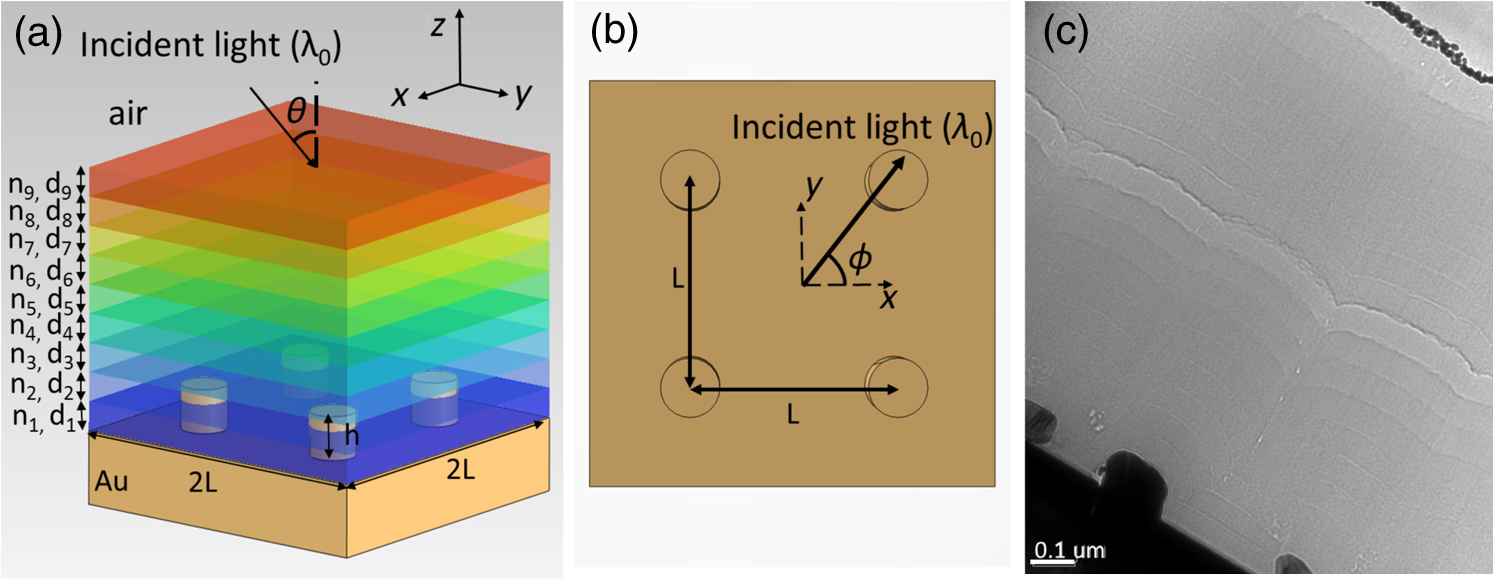 The grating has a period in both the and directions. Each square unit cell of the grating contains a circular step of height of 90 nm and cross-sectional diameter of 190 nm. The complex refractive index of gold, which was calculated from data obtained using an RC2 spectroscopic ellipsometer (Woollam, Lincoln, Nebraska), is presented in Fig. 2. Fig. 2(a) Spectrums of the refractive indices of the nine silicon-oxynitride layers in each period of the 1-D PC. The imaginary parts of the refractive indices were on the order of (Ref. 22) and were therefore ignored. (b) Spectrums of the real and imaginary parts of the refractive index of gold. 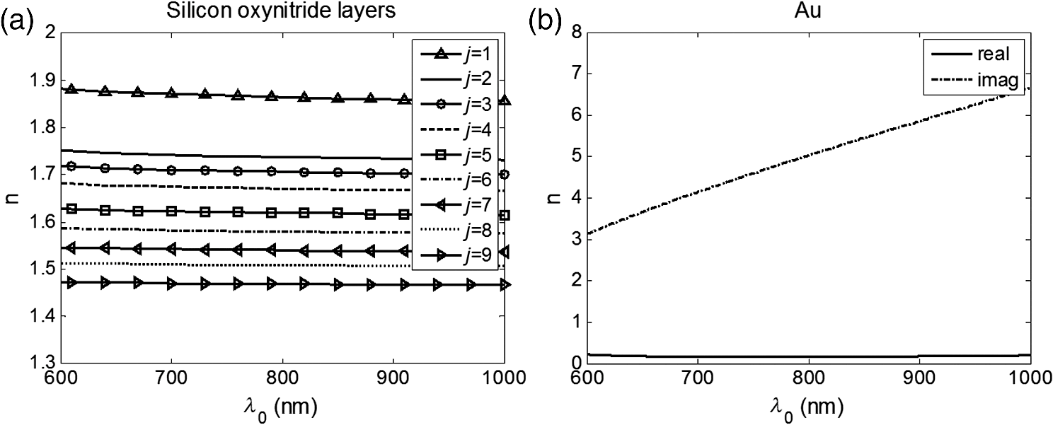 The PC on top of the 2-D gold grating has two periods, although only one period is shown in the figure. Each period consists of nine silicon oxynitride layers of different compositions identified by [0,1]. The silicon oxynitride layers were deposited using plasma-enhanced chemical vapor deposition on a cluster tool (Applied Materials, Santa Clara, California) at a susceptor temperature of 220 °C. Ammonia, silane, and nitrous oxide were used in varying ratios to deposit layers with specific refractive indices. All layers were deposited at a pressure of 3.5 Torr and a power density of . The refractive index of the ’th layer, [1, 9], was measured in the same way as that of the gold layer. The refractive indices of all nine layers are provided in Fig. 2. The transmission-electron microscopy image shown in Fig. 1(c) was used to measure the thickness of the ’th layer, [1, 9]. The measured thicknesses are as follows: , , , , , , and . Let us note that the compositions of the nine layers were merely chosen for ease of fabrication in our nanofabrication facility, and other materials that are virtually nondissipative in the solar spectral regime could be used instead of silicon oxynitride. The specular reflectances and of the structure were measured for [8 deg, 55 deg] and {0 deg,45 deg}, as shown in Figs. 1(a) and 1(b), on a custom spectrometer for incident light of and polarization states, respectively. The measurements were carried for [600, 1000 nm]. A schematic diagram of the custom spectrometer is presented in Fig. 3. A halogen light source (HL-2000, Ocean Optics, Dunedin, Florida) is connected to an optical fiber () (QP400-2-VIS-NIR, Ocean Optics, Dunedin, Florida) which guides light toward a linear polarizer (GT10, ThorLabs, Newton, New Jersey) and an aperture (D20S, Thorlabs, Newton, New Jersey) to be incident on the sample. The reflected light is collected by another optical fiber () (FT600EMT, Thorlabs, Newton, New Jersey) that guides light to a charge-coupled device spectrometer (HRS-BD1-025, Mightex Systems, Pleasanton, California). The sample is mounted on a rotatable stage that controls the incidence angle and the collecting end of is mounted on a rotatable arm that moves to the angle to collect the specularly reflected light. The total transmittance of the structure is null valued in the chosen spectral regime because the metal is thicker than the penetration depth, which was experimentally verified as well. In addition, all nonspecular reflectances are also null valued for the chosen values of , , and . Therefore, the corresponding absorptances of the structure can be calculated as . The measured values of the absorptances and are presented and discussed in Sec. 4.2. 3.Theory in Brief3.1.Surface-Plasmon-Polariton WavenumbersThe SPP wavenumbers were obtained by solving a canonical boundary-value problem.13,19 Suppose the half space is occupied by a metal and the half space by the 1-D PC. The interface can guide the propagation of an SPP wave parallel to the unit vector such that , the associated fields varying in the plane as , where the Cartesian unit vectors are denoted by , etc. The dependences of the fields on are in consonance with the Floquet theory, but are too complicated to be discussed here.19 The procedure to determine is described in detail elsewhere.13,19 Let us note that (1) does not depend on the direction of since all materials are isotropic and the structure is transversely isotropic with respect to the axis and (2) multiple values of for any specific are possible. 3.2.Wavenumbers of Waveguide ModesAs the 1-D PC is thicker than the free-space wavelength [600, 1000 nm], it supports multiple waveguide modes that trap light and play a very significant light-management role for solar-harvesting applications.16–18,24 The wavenumbers of these modes can be obtained using a transfer–matrix approach27 that yields the following matrix equation for a two-period PC bounded by air on one of its two faces and a perfect electric conductor (PEC) on its other face: Here, the matrices where is the angular frequency and is the speed of light in free space; is the permittivity, is the permeability, and is the intrinsic impedance, of free space; is either positive real or positive imaginary; while and are the complex amplitudes of the and -polarized planewave components of light in the air side of the PC. The replacement of gold by a PEC is a reasonable simplification. Equation (1) can be cast as an eigenvalue problem to yield the wavenumbers of - and -polarized waveguide modes.3.3.Predictions for a One-Dimensional Photonic Crystal atop a Two-Dimensional Metal GratingAccording to the Floquet theory,28,29 when a plane wave is incident on a finitely thick 1-D PC atop a 2-D metal grating, all fields must be decomposed everywhere in terms of Floquet harmonics. For the problem under consideration here, a Floquet harmonic of order varies with respect to and as , where and ; see Chap. 3 of Ref. 19. An SPP wave or a waveguide mode with wavenumber is excited as a Floquet harmonic of order , provided that 4.Results and Discussion4.1.Theoretical Results and PredictionsThe normalized wavenumbers of SPP waves guided by a planar metal-PC interface are presented in Fig. 4 as functions of . These wavenumbers are organized in this figure into three branches for -polarized SPP waves and two branches for -polarized SPP waves. Fig. 4(a) Real and (b) imaginary parts of the normalized wavenumbers of surface-plasmon-polariton (SPP) waves obtained after solving the canonical boundary-value problem.  The normalized wavenumbers of the waveguide modes in the air/2-period-PC/PEC structure are presented in Fig. 5. These waveumbers are organized into five branches for -polarized waveguide modes and four branches for -polarized waveguide modes. We inserted the values of provided in Fig. 4 for SPP waves and in Fig. 5 for waveguide modes, and determined that the triplets that would satisfy Eq. (3) for each value of when {0 deg, 45 deg}. Of course, a triplet can be considered as physically acceptable only if . The results are plotted in Fig. 6 for [600, 1000 nm], where the branches indicate the conditions (i.e., the values of and ) at which the SPP and waveguide modes can be excited. It is possible for a specific SPP wave or waveguide mode to be excited as two different Floquet harmonics at the same value of ; likewise, it is also possible for an SPP wave or waveguide mode of a specific polarization state to be excited by incident light of a different polarization state.19 4.2.Experimental Results and Correlation with PredictionsAs stated in Sec. 2, we measured the specular reflectances and of the fabricated structure for [600, 1000 nm], [8 deg, 45 deg], and {0 deg, 45 deg}. Figure 7 presents the color maps of the absorptances and as functions of and for the two chosen values of . Higher absorptances are shown as reddish colors, lower absorptances are shown as bluish colors. The color maps show broadband light absorption over the chosen range of , and we clearly observe reddish ridges of high absorptance corresponding to the excitation of SPP waves and waveguide modes. Overall, the high-absorptance ridges overlay with the theoretically predicted curves in Fig. 6. However, one SPP wave is not observed in our experimental plots and the positions of some of the high-absorptance ridges are slightly shifted from our theoretically predicted curves. These discrepancies might be due to the distortion of the silicon-oxynitide layers in the fabricated structure. This is because these layers are conformally coated on the grating and are not necessarily perfectly planar. Another possible reason for the discrepancies is that some SPP waves are less localized than others and require that the 1-D PC be more than two periods in thickness. On comparing our theoretical and experimental results with those for the 1-D grating,22 we find that the 2-D grating indeed leads to the excitation of more guided waves. We observe broader-band light absorption (high absorptance for ) which is less sensitive to the incidence angle . The structure shows similar light-coupling characteristics for incident - and -polarized light, indicating that the absorption in the structure with a 2-D grating is less dependent on the polarization state of the incident light. A comparison of the results of and reveals that a rotation of the structure about the axis will not greatly influence the absorption of light. Accordingly, the use of 2-D gratings instead of 1-D gratings as metallic back-reflectors should be more efficient for harvesting solar energy. 5.Concluding RemarksWe deposited a 1-D photonic crystal on top of a 2-D metal grating. The absorptances of this structure for incident - and -polarized light were measured and mapped against the free-space wavelength and the incidence angle with respect to the thickness direction. The Floquet theory,28,29 surface-multiplasmonics theory,19 and the transfer–matrix approach for multilayered waveguides27 were used to predict the excitations of SPP waves and waveguide modes as Floquet harmonics. The excitations of guided waves of both types were found to agree well with theoretical predictions. Both the theoretical and experimental results demonstrated broadband coupling of light of any linear polarization state over a broad range of the angles of incidence. Thus, the fabricated structure can be potentially useful as a planar solar concentrator,24 and our light-management approach will also be applicable to thin-film solar cells.23 AcknowledgmentsThis paper is substantially based on a paper titled “Excitation of multiple surface-plasmon-polariton waves and waveguide modes in a 1-D photonic crystal atop a 2-D metal grating,” presented at the SPIE Conference 9191 Nonimaging Optics: Efficient Design for Illumination and Solar Concentration XI, held August 17–21, 2014, in San Diego, California, United States. This work was supported in part by the National Science Foundation under Grant No. DMR-1125591. Fabrication experiments were performed at the Pennsylvania State University Materials Research Institute Nanofabrication Laboratory, which is supported by the National Science Foundation under Cooperative Agreement No. ECS-0335765. AL is grateful to the Charles Godfrey Binder Endowment at Penn State for ongoing support of his research. ReferencesS. A. Maier, Plasmonics: Fundamentals and Applications, Springer, Heidelberg
(2007). Google Scholar
J. Homola, S. S. Yee and G. Gauglitz,
“Surface plasmon resonance sensors: review,”
Sens. Actuat. B: Chem., 54
(1–2), 3
–15
(1999). http://dx.doi.org/10.1016/S0925-4005(98)00321-9 SABCEB 0925-4005 Google Scholar
I. Abdulhalim, M. Zourob and A. Lakhtakia,
“Surface plasmon resonance for biosensing: a mini-review,”
Electromagnetics, 28
(3), 214
–242
(2008). http://dx.doi.org/10.1080/02726340801921650 ETRMDV 0272-6343 Google Scholar
M. Dandin, P. Abshire and E. Smela,
“Optical filtering technologies for integrated fluorescence sensors,”
Lab Chip, 7
(8), 955
–977
(2007). http://dx.doi.org/10.1039/b704008c LCAHAM 1473-0197 Google Scholar
A. Akbari and P. Berini,
“Schottky contact surface-plasmon detector integrated with an asymmetric metal stripe waveguide,”
Appl. Phys. Lett., 95
(2), 021104
(2009). http://dx.doi.org/10.1063/1.3171937 APPLAB 0003-6951 Google Scholar
S. Mokkapati and K. R. Catchpole,
“Nanophotonic light trapping in solar cells,”
J. Appl. Phys., 112
(10), 101101
(2012). http://dx.doi.org/10.1063/1.4747795 JAPIAU 0021-8979 Google Scholar
Y. Nishijima et al.,
“Near-infrared plasmon-assisted water oxidation,”
J. Phys. Chem. Lett., 3
(10), 1248
–1252
(2012). http://dx.doi.org/10.1021/jz3003316 1948-7185 Google Scholar
S. E. Han and G. Chen,
“Toward the Lambertian limit of light trapping in thin nanostructured silicon solar cells,”
Nano Lett., 10
(11), 4692
–4696
(2010). http://dx.doi.org/10.1021/nl1029804 NALEFD 1530-6984 Google Scholar
L. M. Anderson,
“Harnessing surface plasmons for solar energy conversion,”
Proc. SPIE, 0408 172
–178
(1983). http://dx.doi.org/10.1117/12.935723 PSISDG 0277-786X Google Scholar
P. Sheng, A. N. Bloch and R. S. Stepleman,
“Wavelength-selective absorption enhancement in thin-film solar cells,”
Appl. Phys. Lett., 43
(6), 579
–581
(1983). http://dx.doi.org/10.1063/1.94432 APPLAB 0003-6951 Google Scholar
C. Heine and R. H. Morf,
“Submicrometer gratings for solar energy applications,”
Appl. Opt., 34
(14), 2476
–2482
(1995). http://dx.doi.org/10.1364/AO.34.002476 APOPAI 0003-6935 Google Scholar
M. G. Deceglie et al.,
“Design of nanostructured solar cells using coupled optical and electrical modeling,”
Nano Lett., 12
(6), 2894
–2900
(2012). http://dx.doi.org/10.1021/nl300483y NALEFD 1530-6984 Google Scholar
M. Faryad and A. Lakhtakia,
“On surface plasmon-polariton waves guided by the interface of a metal and a rugate filter with a sinusoidal refractive-index profile,”
J. Opt. Soc. Am. B, 27
(11), 2218
–2223
(2010). http://dx.doi.org/10.1364/JOSAB.27.002218 JOBPDE 0740-3224 Google Scholar
N. S. Kapany and J. J. Burke, Optical Waveguides, Academic Press, New York
(1972). Google Scholar
A. W. Snyder and J. D. Love, Optical Waveguide Theory, Chapman and Hall, New York
(1983). Google Scholar
F.-J. Haug et al.,
“Excitation of guided-mode resonances in thin film silicon solar cells,”
Mater. Res. Soc. Symp. Proc., 1321
(1), 123
–128
(2011). http://dx.doi.org/10.1557/opl.2011.946 MRSPDH 0272-9172 Google Scholar
J. R. Nagel,
“Advanced methods for light trapping in optically thin silicon solar cells,”
University of Utah,
(2011). Google Scholar
T. Khaleque and R. Magnusson,
“Light management through guided-mode resonances in thin-film silicon solar cells,”
J. Nanophotonics, 8
(1), 083995
(2014). http://dx.doi.org/10.1117/1.JNP.8.083995 JNOACQ 1934-2608 Google Scholar
J. A. PoloJr., T. G. Mackay and A. Lakhtakia, Electromagnetic Surface Waves: A Modern Perspective, Elsevier, Waltham
(2013). Google Scholar
Devender, D. P. Pulsifer and A. Lakhtakia,
“Multiple surface plasmon polariton waves,”
Electron. Lett., 45
(22), 1137
–1138
(2009). http://dx.doi.org/10.1049/el.2009.2049 ELLEAK 0013-5194 Google Scholar
A. Lakhtakia, Y.-J. Jen and C.-F. Lin,
“Multiple trains of same-color surface plasmon-polaritons guided by the planar interface of a metal and a sculptured nematic thin film. Part III: Experimental evidence,”
J. Nanophotonics, 3
(1), 033506
(2009). http://dx.doi.org/10.1117/1.3249629 JNOACQ 1934-2608 Google Scholar
A. S. Hall et al.,
“Broadband light absorption with multiple surface plasmon polariton waves excited at the interface of a metallic grating and photonic crystal,”
ACS Nano, 7
(6), 4995
–5007
(2013). http://dx.doi.org/10.1021/nn4003488 1936-0851 Google Scholar
M. Faryad et al.,
“Optical and electrical modeling of an amorphous-silicon tandem solar cell with nonhomogeneous intrinsic layers and a periodically corrugated back-reflector,”
Proc. SPIE, 8823 882306
(2013). http://dx.doi.org/10.1117/12.2024712 PSISDG 0277-786X Google Scholar
M. E. Solano et al.,
“Periodically multilayered planar optical concentrator for photovoltaic solar cells,”
Appl. Phys. Lett., 103
(19), 191115
(2013). http://dx.doi.org/10.1063/1.4829641 APPLAB 0003-6951 Google Scholar
106
(7), 079901
(2015). http://dx.doi.org/10.1063/1.4913269 APPLAB 0003-6951 Google Scholar
J. Homola, I. Koudela and S. S. Yee,
“Surface plasmon resonance sensors based on diffraction gratings and prism couplers: sensitivity comparison,”
Sens. Actuat. B: Chem., 54
(1–2), 16
–24
(1999). http://dx.doi.org/10.1016/S0925-4005(98)00322-0 SABCEB 0925-4005 Google Scholar
F. O. Goodman,
“Scattering of atoms by a stationary sinusoidal hard wall: rigorous treatment in (n+1) dimensions and comparison with the Rayleigh method,”
J. Chem. Phys., 66
(3), 976
–982
(1977). http://dx.doi.org/10.1063/1.434007 JCPSA6 0021-9606 Google Scholar
J. Chilwell and I. Hodgkinson,
“Thin-films field-transfer matrix theory of planar multilayer waveguides and reflection from prism-loaded waveguides,”
J. Opt. Soc. Am. A, 1
(7), 742
–753
(1984). http://dx.doi.org/10.1364/JOSAA.1.000742 JOAOD6 0740-3232 Google Scholar
P. C. Waterman,
“Scattering by periodic surfaces,”
J. Acoust. Soc. Am., 57
(4), 791
–802
(1975). http://dx.doi.org/10.1121/1.380521 JASMAN 0001-4966 Google Scholar
A. Lakhtakia, V. K. Varadan and V. V. Varadan,
“Scattering by a partially illuminated, doubly periodic, doubly infinite surface,”
J. Acoust. Soc. Am., 77
(6), 1999
–2004
(1985). http://dx.doi.org/10.1121/1.391771 JASMAN 0001-4966 Google Scholar
BiographyLiu Liu received his BS degree in optical science and engineering from Fudan University, Shanghai, China, in 2010. He is now pursuing a doctorate in electrical engineering at The Pennsylvania State University. His current research interests include plasmonics and advanced optical materials. Muhammad Faryad received his MSc and MPhil degrees in electronics from Quaid-i-Azam University in 2006 and 2008, and his PhD degree in engineering science and mechanics from The Pennsylvania State University in 2012, where he also served as a postdoctoral research scholar until 2014. He is now an assistant professor of physics at the Lahore University of Management Sciences, Pakistan. His research interests include modeling of thin-film solar cells, electromagnetic surface waves, and sculptured thin films. Anthony Shoji Hall received his BS in chemistry from UCLA in 2010 and his PhD in chemistry from The Pennsylvania State University in 2014. Currently, he is a postdoctoral research fellow at Massachussetts Institute of Technology in the Department of Chemistry. His research focuses broadly on the application of ordered mesoporous materials for electrochemical fuel production. Greg D. Barber received his BS degrees in physics and ceramic science and engineering in 1991, and his MS and PhD degrees in materials science from The Pennsylvania State University in 1995 and 1998. Currently, he is a research associate in the Penn State Institute for Energy and the Environment. His research focuses on solar radiation, thin-film solar materials, carbon, and inorganic materials systems with particular emphasis on materials chemistry and scalable materials processing. Sema Erten received her BS degree in engineering physics from Hacettepe University, Ankara, Turkey, and her MS degree in engineering science from The Pennsylvania State University. She is now pursuing a doctorate in engineering science and mechanics at Penn State. Her current research interests include sculptured thin films and nanophotonics. Thomas E. Mallouk is an Evan Pugh professor with joint appointments in the Departments of Chemistry, Physics, and Biochemistry and Molecular Biology at The Pennsylvania State University. He received his ScB degree in chemistry from Brown University in 1977, and his PhD degree in chemistry from the University of California, Berkeley, in 1983. His research focuses on the application of nanomaterials to problems in solar energy conversion, catalysis and electrocatalysis, motion on the nanoscale, and environmental remediation. Akhlesh Lakhtakia is the Charles Godfrey Binder (Endowed) professor of engineering science and mechanics at The Pennsylvania State University. He is a fellow of SPIE, OSA, American Association for the Advancement of Science, American Physical Society, and Institute of Physics (UK). He was the sole recipient of the 2010 SPIE Technical Achievement Award. His current research interests include sculptured thin films, mimumes, electromagnetic surface waves, thin-film solar cells, bone refacing, bioreplication, and forensic science. Theresa S. Mayer received her BS degree in electrical engineering from Virginia Tech in 1988, and her MS and PhD degrees in electrical engineering from Purdue University in 1989 and 1993. She is a distinguished professor of electrical engineering and materials science and engineering at Penn State University. Her research focuses on adding new functionality to silicon integrated circuits and on creating engineered nanostructures with artificial electrical and optical properties. |