|
|
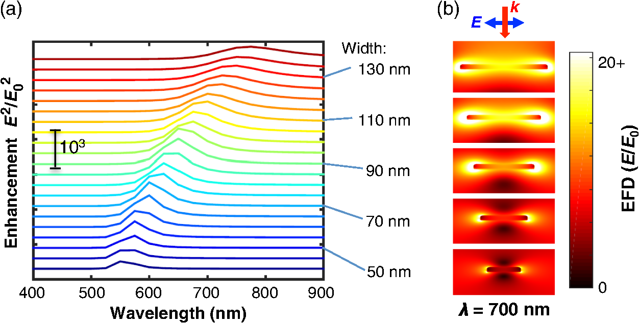
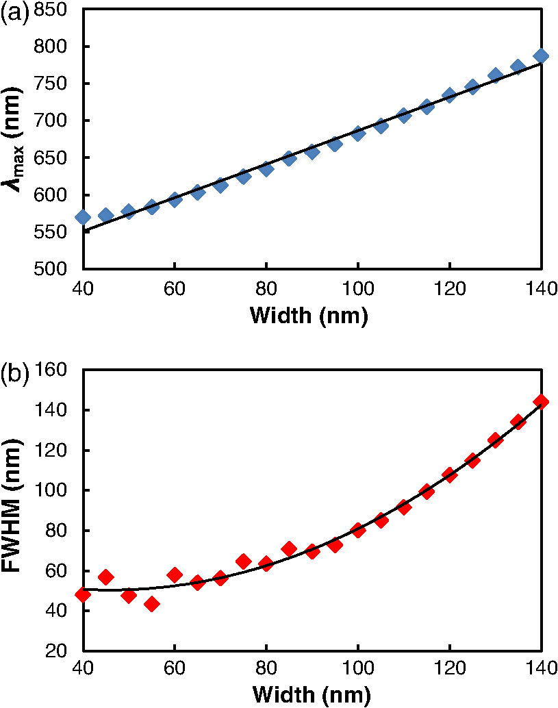
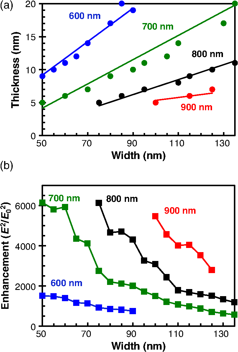
1.IntroductionWhen an electromagnetic wave is incident on a metal surface, it will cause an oscillation of the free electron density of the metal. The oscillation of these electrons is quantized, and this quantization of plasma oscillations is called a plasmon.1 Because plasmons are a quantization of plasma oscillations, their properties can be derived from Maxwell’s equations.2 The usefulness of plasmons is exhibited by their ability to localize light to scales much smaller than the diffraction limit3 and amplify the magnitude of the electric field in plasmonic nanostructures to many times more than the incident electric field. The optical response of plasmonic structures exhibit dependence on the polarization direction,4 incident wavelength, and nanostructure geometry,3 so the maximum possible electric field amplification will vary for any given plasmonic coupling conditions. The importance in the proper tuning of plasmonic properties becomes apparent in the wide variety of possible applications for plasmonic devices, such as enhanced photovoltaics,5,6 biosensing,7 surface-enhanced Raman spectroscopy,8 enhanced photodetectors,6,9–11 thermoplasmonic applications,12–14 and photothermal therapy.15–18 These applications have potentially significant impact across many societally important issues from improved energy production to medical treatment. This work will investigate the effect of various cross-sectional geometries of gold nanowires in order to maximize the achievable optical enhancement. Similar goals have been presented in the previous work,17,19 but are more specific in scope or differ in the investigated geometry. This work attempts to find a general relationship between nanowire cross-sectional geometry and optical enhancement. The geometries under investigation in this work focused on typical nanowire dimensions that can be fabricated with electron beam lithography (EBL). Additionally, a model was created here to investigate the effects of nanogaps between parallel gold nanowires to study the effects of gap enhancement20 as a function of various nanowire dimensions. 2.MethodsOptical studies have been performed on single nanowires and an array of three parallel nanowires separated by nanogaps: a triple nanowire array. Finite element method (FEM, COMSOL) simulations have been used to determine the plasmonic response of metallic nanostructures to incident electromagnetic waves. The simulations are performed in a two-dimensional (2-D) simulation space, which approximates the nanowires as infinitely long with a rectangular cross section. Full simulation geometry details are described in the Appendix. Substrate effects have been approximated by using an effective medium of in the space surrounding the nanowires.8,14,21 This approximation is useful in modeling plasmonic structures fabricated with EBL on silicon substrates with a silicon oxide layer. The material properties of gold are applied to the nanowires and are modeled using an experimentally derived dielectric function.22 An electromagnetic wave has normal incidence to the top surface of the nanowire and is transversely polarized (the electric field is polarized across the width of the nanowire) for each simulation. Transverse polarization is used because we are varying the transverse width of the nanowire in the model. Each simulation reports a plot of the electric field distribution (EFD), defined as , where is the local electric field of the plasmonic nanostructure and is the incident electric field. Therefore, the EFD is the ratio of the local electric field to the incident electric field. A number also of interest is the optical enhancement, defined as (or the EFD squared), which is a measure of the increase in local intensity, as intensity is proportional to the electric field squared: . The enhancement values reported in this work represent the maximum enhancement value for a particular simulation, which is located in the region close to the nanowire sidewalls, as shown in Fig. 1(b). 3.Results and Discussion3.1.Single Nanowire Width DependenceFirst, the dependence of enhancement on the width of the nanowire was determined. The enhancement spectra for various widths are plotted in the waterfall plot of Fig. 1(a). These are the maximum optical enhancement values of a single gold nanowire as a function of the wavelength of the light incident on the structure. Each line on the plot represents a different simulation for a particular width. The nanowire thickness remains fixed at 15 nm and the width ranges from 40 to 140 nm, with a step size of 5 nm between each width. Figure 1(a) shows that the enhancement peak shifts toward the red as nanowire width increases. Figure 1(b) is a cross-sectional view of the EFDs to demonstrate the enhancement patterns as a function of width for a constant wavelength of 700 nm. Figure 2(a) plots the incident wavelength that provides the maximum optical enhancement for a particular nanowire width. The values in Fig. 2(a) are obtained from Fig. 1(a). The simulation results in Fig. 1(a) were fitted with a first-order Gaussian function. The coefficients for the best-fit Gaussian function were then used to determine the peak enhancement wavelength. The results show a linearly increasing relationship. This corresponds to the fact that the transversely polarized incident light excites the transverse plasmonic mode, which oscillates across the horizontal surfaces of the cross section. As the nanowire width increases, the transverse plasmon couples efficiently with larger wavelengths. Figure 2(b) plots the full width at half maximum of the broadening in the enhancement spectrum as nanowire width increases. As can be seen from the plot, the broadening exhibits a quadratic proportionality to the width of the nanowire. The enhancement spectral peak broadens as the width increases because the plasmon resonance also broadens as size increases for structures that are greater than 40 nm. This is due to the larger structures having multipolar plasmons that can couple with a broader range of wavelengths and due to additional electron damping caused by secondary radiation from accelerated electrons.23,24 3.2.Triple Nanowire ArrayThe next simulations model the three nanowires in parallel separated by nanogaps. The geometry is motivated by nanogap plasmonic structures that can be fabricated by the nanomasking technique.25 Figure 3(a) identifies the geometric parameters that were investigated for the triple nanowire array. The outer two nanowires have the same width, denoted , which is shorter than the width of the center nanowire, denoted . Figures 3(b)–3(d) are EFDs for several unique simulations. For the three simulations shown, the incident wavelength, gap width, and nanowire thickness remain constant at values of 700, 5, and 15 nm, respectively. The difference between each simulation is the width of the nanowires, indicated at the top of each EFD. This figure shows that the optical enhancement is concentrated in the gaps between the nanowires and also at the corners of each nanowire. Another observation of significance is the substantial difference in gap enhancement for varying nanowire widths, such as seen between Figs. 3(b) and 3(d). In this case, a substantial increase [from Figs. 3(d) to 3(b)] in optical enhancement is seen for a difference in of only 20 nm. Fig. 3(a) Triple nanowire array cross-section geometry showing the incident light direction and polarization (b–d) EFDs of triple nanowire arrays with various geometries. The maximum EFD achieved in these simulations was approximately 37.24. 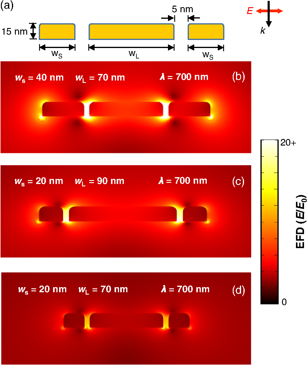 Figures 4(a)–4(d) plot the maximum optical enhancement for each unique and combination for incident wavelengths of 600, 700, 800, and 900 nm. The width ranges from 10 to 90 nm while ranges from 40 to 140 nm, both with a step size of 10 nm. The intensity profile follows a roughly negative linear pattern for all wavelengths. The negative linear relationship shown in Fig. 4 [and also Fig. 5(b)] could be due to a plasmonic coupling between the nanowires resulting in an effective overall width of the array structure. Fig. 4Maximum enhancement of triple nanowire array as a function of and for four different wavelengths. The maximum enhancement achieved in these simulations was approximately 1387. 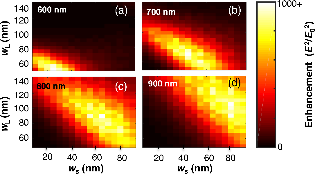 Fig. 5(a) Maximum enhancement at optimal as a function of . (b) that gives maximum enhancement as a function of for triple nanowire array. Data points are individual simulation results, and the line is fitting obtained from Eq. (3). 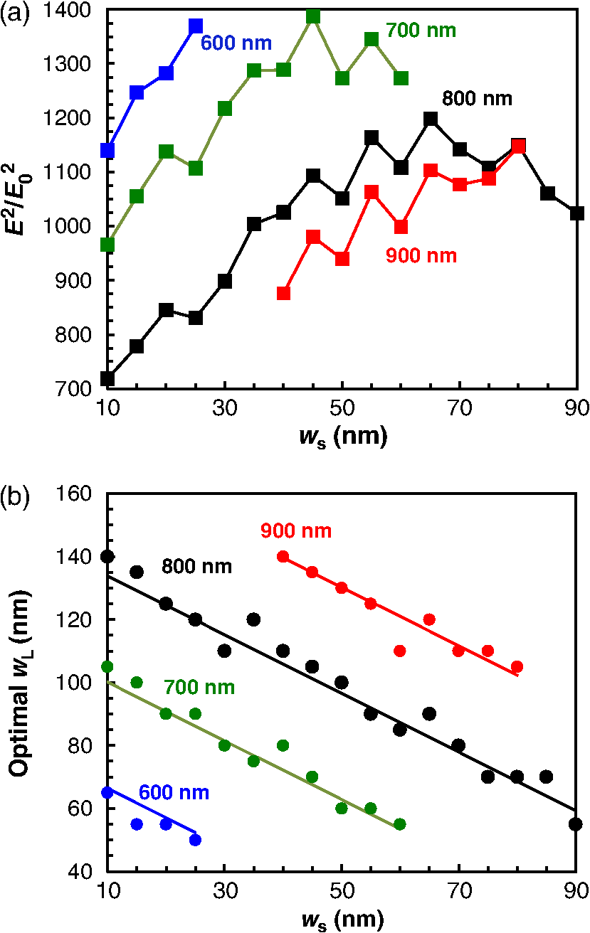 Figure 5(a) plots the maximum optical enhancement that was obtained as a function of . The peak of the optical enhancement curves strongly shifts to higher for increasing wavelength and reaches a maximum value of approximately 1387 for a wavelength of 700 nm. Figure 5(b) plots the that provides the maximum optical enhancement as a function of , which shows a linear relationship. The range of points plotted differs for each wavelength due to shifts in the enhancement patterns that can be shown in Figs. 4(a)–4(d). The slope values obtained for 600, 700, 800, and 900 nm wavelengths are , , , and with vertical intercept () 72, 113, 147, and 173 nm, respectively. In order to develop a general equation to determine the optimal for maximum enhancement based on wavelength and , a general function was considered. Based on the similarity in slope between each line, and the roughly linear relationship between their vertical intercepts, the general function can be rewritten as where is the average slope of the enhancement for each spectra and is calculated from the vertical intercept values . The vertical intercept as a function of wavelength is given by , where and the constant is extrapolated from observed values. Substituting the calculated values into Eq. (1), one obtainsThe solid lines in Fig. 5(b) are plots of Eq. (3) for each wavelength. Equation (3) is a useful result that can be used to design a structure with appropriate parameters (, , or ) to maximize the optical enhancement of a gold nanowire array if the other two variables are defined. As can be shown in Fig. 5(b), Eq. (3) is a good estimation of the optimum value of for the plotted data. 3.3.Thickness DependenceNext, the effects of nanowire thickness were investigated. Figure 6 displays simulation results in the form of EFDs, each corresponding to a different nanowire thickness. For each simulation, the wavelength and nanowire width remain constant: and . These plots show that there is a significant difference in the optical enhancement as the thickness changes, as can most clearly be seen between the EFDs for nanowire thicknesses of 5 and 11 nm. This is potentially due to effects of vertical plasmonic modes26 that oscillate vertically along the side surfaces of the cross section of the nanowire. Fig. 6EFDs of single nanowires of varying thickness. The maximum EFD achieved in these simulations was approximately 78.4. 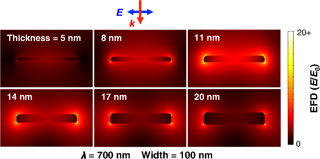 Figures 7(a)–7(d) correspond to simulations of a single nanowire, and plot the maximum optical enhancement as a function of nanowire thickness and width for incident wavelengths of 600, 700, 800, and 900 nm. The slope of the maximum enhancement line changes between each wavelength, though it remains positive in each case. Additionally, as wavelength increases, the maximum enhancement at lower nanowire thickness shifts toward larger widths. Fig. 7Maximum optical enhancement as a function of width and thickness for a single nanowire for four different wavelengths. The maximum enhancement achieved in these simulations was approximately 6147. 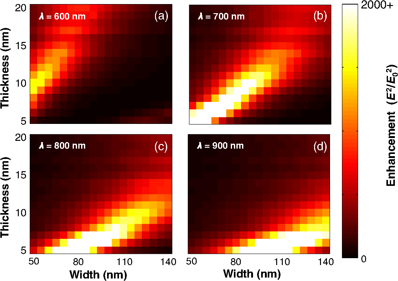 Figure 8(a) plots the thickness that provides the maximum enhancement as a function of width, similar to how Fig. 5(b) demonstrated this for widths. Again, the range of points on each line is limited by the range that was calculated and due to shifts in the enhancement pattern that can be shown in Figs. 7(a)–7(d). Figure 8(a) more clearly demonstrates the shift in the slope of the enhancement pattern between each wavelength. The slope values obtained for 600, 700, 800, and 900 nm wavelengths are 0.285, 0.167, 0.099, and 0.079, respectively. Using the same method as for the first equation, the first step in developing a general equation is where is the nanowire thickness that will produce the maximum enhancement for a specific nanowire width and incident wavelength . Since the slope is different for each wavelength, it must be represented as a function of wavelength rather than an average where is an intercept interpolated from the data. The slope as a function of wavelength is given by: , where and the constant is extrapolated from observed values. Combining the above values with Eq. (5) yields In Eq. (6), is a constant that differs between wavelengths, and is adjusted between and 5 nm to fit Eq. (6) to the data. The solid lines in Fig. 8(a) are plotted using Eq. (6). Another useful relationship between , , and has been determined. This result can be used to optimize the design parameters to maximize the optical enhancement of a single gold nanowire. Figure 8(b) plots the maximum enhancement for each width, where the thickness is the one that provides the highest enhancement for the given width. The plot shows that the maximum optical enhancement peak shifts to the right for increasing wavelength, in a fairly consistent step size of . The enhancement reaches a maximum value of approximately 6147 for a wavelength of 700 nm for the specific thickness and width ranges.4.ConclusionsThis work investigated the optical enhancement properties of gold nanowires using a 2-D FEM analysis. For a nanowire with constant thickness of 15 nm, a relationship between wavelength and cross-sectional width has been determined for transversely polarized incident light. A relationship has been determined [Eq. (3)] for three parallel gold nanowires. Finally, a thorough investigation of the dependency of optical enhancement on nanowire width and thickness has been completed. The relationship between these parameters has been found for the tested geometries [Eqs. (3) and (6)] and can serve as a useful tool to researchers as they design and fabricate plasmonic nanostructures. As the control provided by various nanostructure fabrication methods advances, it will become increasingly necessary to appropriately tune the geometry of plasmonic nanostructures in order to maximize their effectiveness in any given application, as has been demonstrated in the previous work.17,19 Therefore, as future research continues to push the fabrication of plasmonic nanostructures, the relationship between nanowire thickness and width will be a valuable resource. AppendicesAppendix:Simulation DetailsSimulation geometry is shown in Fig. 9. The nanowire is at the center of the 2-D simulation space and the cross section is shown. The top edges of the cross section of the nanowire are beveled to provide a closer approximation to an actual nanowire fabricated with EBL. Surrounding the nanowire is a circle of radius 1100 nm, split into two distinct layers: the far-field domain, an 800-nm radius inner layer, the perfectly matched layer (PML), a 300-nm outer layer. The far-field domain represents the air through which the electromagnetic wave propagates before it interacts with the nanowires. The effective medium, , is applied to the far-field domain to model the properties of air along with the substrate. AcknowledgmentsFunding has been provided in part by the National Science Foundation Grant Award No. 1359306. ReferencesJ. B. Pendry et al.,
“Extremely low frequency plasmons in metallic mesostructures,”
Phys. Rev. Lett., 76
(25), 4773
–4776
(1996). http://dx.doi.org/10.1103/PhysRevLett.76.4773 PRLTAO 0031-9007 Google Scholar
S. A. Maier, Plasmonics: Fundamentals and Applications, Springer Science + Business Media LLC, Dordrecht, Netherlands
(2007). Google Scholar
D. K. Gramotnev and S. I. Bozhevolnyi,
“Plasmonics beyond the diffraction limit,”
Nat. Photonics, 4 83
–91
(2010). http://dx.doi.org/10.1038/nphoton.2009.282 Google Scholar
H. Wei et al.,
“Polarization dependence of surface-enhanced Raman scattering in gold nanoparticle–nanowire systems,”
Nano Lett., 8
(8), 2497
–2502
(2008). http://dx.doi.org/10.1021/nl8015297 NALEFD 1530-6984 Google Scholar
H. A. Atwater and A. Polman,
“Plasmonics for improved photovoltaic devices,”
Nat. Mater., 9 205
–213
(2010). http://dx.doi.org/10.1038/nmat2629 NMAACR 1476-1122 Google Scholar
E. T. Yu et al.,
“Plasmonic nanoparticle scattering for enhanced performance of photovoltaic and photodetector devices,”
Proc. SPIE, 7033 70331V
(2008). http://dx.doi.org/10.1117/12.798327 PSISDG 0277-786X Google Scholar
J. N. Anker et al.,
“Biosensing with plasmonic nanosensors,”
Nat. Mater., 7 442
–453
(2008). http://dx.doi.org/10.1038/nmat2162 NMAACR 1476-1122 Google Scholar
J. B. Herzog et al.,
“Dark plasmons in hot spot generation and polarization in interelectrode nanoscale junctions,”
Nano Lett., 13
(3), 1359
–1364
(2013). http://dx.doi.org/10.1021/nl400363d NALEFD 1530-6984 Google Scholar
W. Wu, A. Bonakdar and H. Mohseni,
“Plasmonic enhanced quantum well infrared photodetector with high detectivity,”
Appl. Phys. Lett., 96 161107
(2010). http://dx.doi.org/10.1063/1.3419885 APPLAB 0003-6951 Google Scholar
A. M. Hill et al.,
“Computational electromagnetic analysis of plasmonic effects in interdigital photodetectors,”
Proc. SPIE, 9163 91633Q
(2014). http://dx.doi.org/10.1117/12.2074251 PSISDG 0277-786X Google Scholar
A. I. Nusir et al.,
“Near-infrared metal–semiconductor–metal photodetector based on semi-insulating GaAs and interdigital electrodes,”
Photonics Res., 3 1
–4
(2015). http://dx.doi.org/10.1364/PRJ.3.000001 Google Scholar
M. Zhu et al.,
“Micropatterning thermoplasmonic gold nanoarrays to manipulate cell adhesion,”
ACS Nano, 6
(8), 7227
–7233
(2012). http://dx.doi.org/10.1021/nn302329c ANCAC3 1936-0851 Google Scholar
R. Rodríguez-Oliveros and J. A. Sánchez-Gil,
“Gold nanostars as thermoplasmonic nanoparticles for optical heating,”
Opt. Express, 20 621
–626
(2012). http://dx.doi.org/10.1364/OE.20.000621 OPEXFF 1094-4087 Google Scholar
J. B. Herzog et al.,
“Thermoplasmonics: quantifying plasmonic heating in single nanowires,”
Nano Lett., 14
(2), 499
–503
(2014). http://dx.doi.org/10.1021/nl403510u NALEFD 1530-6984 Google Scholar
X. Huang et al.,
“Plasmonic photothermal therapy (PPTT) using gold nanoparticles,”
Lasers Med. Sci., 23 217
–228
(2008). http://dx.doi.org/10.1007/s10103-007-0470-x Google Scholar
X. Huang and M. A. El-Sayed,
“Plasmonic photo-thermal therapy (PPTT),”
Alex. J. Med., 47 1
–9
(2011). http://dx.doi.org/10.1016/j.ajme.2011.01.001 Google Scholar
M. A. Mackey et al.,
“The most effective gold nanorod size for plasmonic photothermal therapy: theory and in vitro experiments,”
J. Phys. Chem. B, 118 1319
–1326
(2014). http://dx.doi.org/10.1021/jp409298f JPCBFK 1520-6106 Google Scholar
Y. H. Wang et al.,
“Synergistic delivery of gold nanorods using multifunctional microbubbles for enhanced plasmonic photothermal therapy,”
Sci. Rep., 4 1
–8
(2014). http://dx.doi.org/10.1038/srep05685 SRCEC3 2045-2322 Google Scholar
S. Yun et al.,
“Linker-molecule-free gold nanorod films: effect of nanorod size on surface enhanced Raman scattering,”
J. Phys. Chem. C, 113 13551
–13557
(2009). http://dx.doi.org/10.1021/jp9024624 JPCCCK 1932-7447 Google Scholar
D. Natelson, Y. Li and J. B. Herzog,
“Nanogap structures: combining enhanced Raman spectroscopy and electronic transport,”
Phys. Chem. Chem. Phys., 15 5262
–5275
(2013). http://dx.doi.org/10.1039/c3cp44142c PPCPFQ 1463-9076 Google Scholar
T. C. Choy, Effective Medium Theory: Principles and Applications, Oxford University Press, Oxford, England
(1999). Google Scholar
P. B. Johnson and R. W. Christy,
“Optical constants of the noble metals,”
Phys. Rev. B, 6 4370
–4379
(1972). http://dx.doi.org/10.1103/PhysRevB.6.4370 Google Scholar
A. Noguez,
“Surface plasmons on metal nanoparticles: the influence of shape and physical environment,”
J. Phys. Chem. C, 111 3806
–3819
(2007). http://dx.doi.org/10.1021/jp066539m JPCCCK 1932-7447 Google Scholar
A. L. Schmucker et al.,
“Correlating nanorod structure with experimentally measured and theoretically predicted surface plasmon resonance,”
ACS Nano, 4
(9), 5453
–5463
(2010). http://dx.doi.org/10.1021/nn101493t ANCAC3 1936-0851 Google Scholar
A. Sobhani et al.,
“Narrowband photodetection in the near-infrared with a plasmon-induced hot electron device,”
Nat. Commun., 4 1643
(2013). http://dx.doi.org/10.1038/ncomms2642 NCAOBW 2041-1723 Google Scholar
BiographyCameron Saylor will start graduate school in the Physics Department at the University of California, Davis, in 2015. He received his BS degree in physics and mechanical engineering from the University of Arkansas, Fayetteville, USA, in 2015. He is a member of SPIE. Eric Novak will start graduate school in the Materials Science and Engineering Department at the University of Tennessee, Knoxville, USA, in 2015. He received his BS degree in physics from Shippensburg University of Pennsylvania in 2015. His graduate research will focus on neutron spin echo spectroscopy at Oak Ridge National Laboratory. Desalegn Debu is a graduate student in the Physics Department at the University of Arkansas, Fayetteville, USA. He received his MS degree in physics from Addis Ababa University in Ethiopia in 2006, and received his BS degree in physics from Dilla University (Ethiopia) in 2004. Joseph B. Herzog is a visiting assistant professor in the Department of Physics at the University of Arkansas. He received his BS degree in electrical engineering from Louisiana State University and his MS and PhD degrees in EE from the University of Notre Dame in 2011. He was a postdoctoral research associate at Rice University from 2011 to 2013. His research focuses on nano-optics including plasmonics and photonic crystals. He is an active member of SPIE serving on various committees. |