
|
|
1.IntroductionPhotonic crystals (PCs) are receiving attention because of their attractive optical properties. PCs are composed of a periodic array of dielectric mediums with different refractive indices; they can manipulate the propagation of lights with a wavelength-scale structure. PC cavities have been applied to nanolasers,1–6 optical switches,7,8 and single-photon sources9–14 because of their low optical loss and wavelength-sized mode volume, which enables strong light–matter interactions. In particular, the single-photon sources employed for quantum cryptology consist of a high quality factor () PC cavity and a quantum dot (QD) as an atom-like emitter. When the QD is placed at the antinode of the cavity-mode profile and the emission wavelength of the QD is matched with the cavity resonance, the light–matter interactions are maximized and the system of a QD-PC cavity can play the role of an efficient single-photon source. However, since a PC cavity is fabricated by a semiconductor process such as e-beam lithography and etching,2,15 it is not guaranteed that the determined characteristics of the PC cavity, resonant wavelength, and mode profile match the emission wavelength and the position of a QD grown randomly in the wafer. In fact, the operation of a QD-based PC cavity as the single-photon source usually depends on accidentally matching the spectral/spatial position of the QD and the cavity, which makes an applicable single-photon source a very challenging and impractical device. Therefore, a PC cavity that has spatial position flexibility and spectral tenability would be an important milestone for the development of a useful single-photon source. On the other hand, a spatially tunable PC cavity has been reported in which a bent tapered optical fiber is brought close to a PC to form a cavity, while having a limit of mechanically weakness of tapered fiber.16 In our research, we propose a PC cavity that is spatially relocatable and spectrally tunable and analyze properties of the structure by calculating three-dimensional model with finite-differential time-domain method. The proposed PC cavity is composed of a microscale dielectric sphere on a defect-free PC slab. The position of the PC cavity is relocated to a desired point simply by moving the sphere to that point. A resonant wavelength of the PC cavity is also tuned, not only coarsely by modifying parameters of the sphere (e.g., the radius and the refractive index) but also finely by changing the height of the sphere from the PC slab. The single-photon source is simply formed by using the attributes of the proposed PC cavity. 2.Spatial RelocatabilityWhen a microsphere is placed on the PC slab, the effective refractive index near the sphere increases and a localized defect is formed in the PC slab, which works as a PC cavity. The PC composed of a triangular lattice has a periodicity () of 550 nm and an air-hole radius of 192.5 nm (). The slab thickness is 200 nm. The PC slab has a photonic band structure as shown in Fig. 1(b). In the PC structure, the photonic bandgap is from 1309 to 1744 nm. In this study, the investigated radius of the sphere ranges from 1000 to 1600 nm and the refractive index of the sphere is assumed to range from 1.70 to 3.40. Fig. 1(a) Scheme of a tunable PC cavity with a dielectric microsphere and a two-dimensional (2-D) triangular lattice PC slab. The slab index is assumed to be 3.4. Thickness (), lattice constant (), and air-hole radius () are 200, 550, and 192.5 nm, respectively. (b) Photonic band structure of the PC slab. The bandgap is formed from 1309 (blue circle) to 1774 nm (red circle).  The fabrication of the usual PC cavities needs to be state-of-art e-beam lithography or semiconductor etching for patterning a defect in the PC. For example, in an air-hole PC slab, a defect is formed by reducing or removing an air hole because the effective refractive index of the modified hole increases. However, the proposed cavity is formed when a dielectric sphere contacts a defect-free PC slab. In the cavity, no physical defect exists in the PC slab; however, the local index increases due to the existence of a microsphere working like a defect. Therefore, the proposed cavity only needs a noncomplex method such as laser holography for patterning a defect-free PC slab.17,18 In addition, the position and resonant wavelength of the cavity are variable because of their dependency on the parameters of the sphere, such as the position, radius, and refractive index. In order to figure out the cavity modes that are formed by the position of the dielectric microsphere, we investigate the typical positions of the triangular lattice, as shown in Figs. 2(a) and 2(c). First, a microsphere with a radius of 1500 nm and a refractive index of 1.95 is placed on a black spot in Fig. 2(a), which is at the center of the three air holes creating the triangular lattice. This cavity, called a zero-cell cavity,5 has three localized cavity modes, such as a single monopole mode and doubly degenerated dipole modes, as shown in Fig. 2(b). One dipole mode has symmetry along the axis, another has symmetry along the axis. The resonant wavelengths are 1477 nm for the monopole mode and 1476 nm for the degenerated dipole modes. All three modes are strongly localized near the contact position of the microsphere. The factors are 480 and 380 for the monopole and dipole modes, respectively. Fig. 2(a) Microsphere position between the air holes. (b) Mode profiles of tunable PC cavity modes, monopole, dipole 1, and dipole 2 when a microsphere is placed on the black dot in (a). The microsphere has a refractive index, and a radius . (c) Microsphere position at the center of the air hole. (d) Mode profiles of the PC cavity modes, double-degenerated dipoles and quadrupoles, and hexapole when a microsphere is placed on the black dot in (c). The microsphere has a refractive index and a radius .  On the other hand, the PC cavity mode can also be excited when a dielectric microsphere with a radius of 1500 nm and an index of 2.35 is placed at the center of an air hole, as indicated by the black dot in Fig. 2(c). In contrast to this, the sphere makes contact with the surface of the slab in Figs. 2(a) and 2(b), and the sphere is partially inserted inside an air hole (inset). The cavity supports the same PC cavity modes with a single-cell cavity1,3,19 and has doubly degenerated dipole modes, doubly degenerated quadrupole modes, and a single hexapole mode as shown in the mode profiles (Hz field) of Fig. 2(d). The resonant wavelengths are 1616 nm for the dipole modes, 1310 nm for the quadrupole modes, and 1496 nm for the hexapole mode. Since the frequency is placed outside the bandgap, the monopole mode is not observed. The factors are 10,000 for the dipole modes, 1,000 for the quadrupole modes, and 6,800 for the hexapole mode. The hexapole mode has a high factor due to mode cancellation.20,21 Here, the refractive indices, 1.95 (e.g., index of SiN) and 2.35 (e.g., index of ), of the spheres in Figs. 2(a) and 2(c) are chosen for the all presented cavity modes to be well-localized horizontally. Therefore, the cavity mode of the proposed cavity at an arbitrary point is created by setting the sphere on the point. Consequently, the cavity mode is well formed wherever the sphere comes between the air holes or when it is at the center of an air hole with a high factor and wavelength-sized mode volume. In other words, the position of the cavity is relocatable spatially by adjusting one of the spheres. The hexapole mode still has characteristics of the general single-cell mode, e.g., a large value and small mode volume. However, unlike the general single-cell hexapole mode, the hexapole mode created by a sphere can have several resonant wavelengths with an individual azimuthal mode number in the sphere at the -plane, as shown in Fig. 3. For example, the resonance of a hexapole mode is observed at 1357, 1463, 1591, and 1748 nm in the bandgap when the sphere with a 1000-nm radius and 2.91-refractive index makes contact with the slab. Each mode shows the field at the edge of the sphere like the whispering guided mode,22–24 as shown in the mode profile of the cross-section of the -plane [Fig. 3(b)]. The modes can be classified by the number of oscillations in the circumference of the sphere, called the azimuthal mode number. In this case, the azimuthal mode numbers of each mode are 9, 8, 7, and 6. Therefore, the proposed cavity is free to choose the resonant wavelength when the cavity is coupled with an emitter because the resonant wavelength is selected in a large region from 1357 to 1748 nm with the same hexapole mode as the PC. The resonant wavelength decreases when the azimuthal mode number increases.24 Therefore, the hexapole mode excited in the proposed cavity can have four resonant wavelengths distributed from 1357 to 1748 nm over a broad photonic bandgap spectrum while horizontal electric field profiles are maintained. Here, the index of 2.91 of sphere (index of chalcogenide glass) is chosen for the presented four hexapole modes to be well-localized horizontally. 3.Spectral TunabilityWhen the sphere is chosen with a different radius and refractive index, the hexapole mode can be excited at a desired wavelength ranged in 1339 to 1725 nm, where it covers the entire photonic bandgap of the defect-free PC slab. In order to investigate how the resonant wavelength depends on the index and radius of the sphere, we calculated the wavelength of the hexapole mode with azimuthal mode number 8 (Fig. 3) because the resonant wavelength is in the middle of the bandgap. The resonant wavelength can be controlled from 1343 to 1722 nm by changing a refractive index of the sphere from 2.43 to 3.16 with . The resonant wavelength can also be changed from 1339 to 1725 nm by increasing the radius of the sphere from 1000 to 1300 nm with . A similarly large spectral tuning of 400 nm is achievable by selecting a proper radius and index of the sphere. On the other hand, each resonant wavelength can be tuned by changing the index or the radius of the sphere. According to the hexapole mode at the -plane and the azimuthal mode with a mode number of 8 at the -plane, the resonant wavelength and factor are mapped with respect to the refractive index and radius of the sphere. The resonant wavelength increases when the refractive index or the radius of the sphere increases because the size of the effective resonator becomes larger. There is no resonant mode at the white regions in Figs. 4(c) and 4(d). Since it is over the bandgap from 1309 to 1774 nm, light cannot be confined horizontally in the slab. The factor has as the maximum value when the sphere has the refractive index of 1.67 and the radius of 1300 nm. By selecting the index and radius of the sphere, the hexapole mode can be excited with the desired wavelength and factors. However, in applications of the optical filter or quantum optics, fine spectral tuning of the cavity mode after fabrication is also required. Fig. 4Resonant peak of the hexapole mode with an azimuthal mode number of 8 versus the (a) refractive index with fixed radius and (b) radius with fixed refractive index of 2.67. (c) 2-D mapping of resonant wavelengths and (d) factors with respect to radius and refractive index of microsphere. 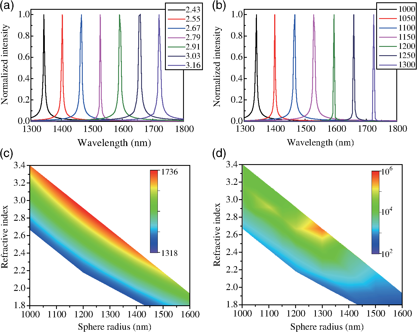 In the proposed cavity, the resonant wavelength selectivity accounts for 300 nm by choosing another azimuthal mode or selecting a sphere with a specific radius and refractive index. After the sphere is determined, the resonant wavelength is still finely tunable by adjusting the height of the sphere from the PC slab. In this resonance structure, the effective index can be decreased by inserting an air gap between the dielectric sphere and the PC slab. A resonant wavelength with the sphere that has and can be controlled by changing the height of the air gap, as shown in Fig. 5. In fact, the resonant wavelength decreases from 1449 to 1444 nm when the air gap increases from 0 to 500 nm. The linewidth of the resonance is 0.45 nm when the air gap is 0 nm because the factor is 3200. Thus, we can observe the 5 nm shift induced by changing the air gap because the amount of resonant peak shifting is greater than the linewidth. Fig. 5(a) Schematic of spectral tuning by moving the sphere vertically. The height of the air gap is measured from the surface of the slab to the sphere. (b) Resonant wavelength as a function of the height of the air gap. The wavelength decreases from 1449 to 1444 nm when the air gap increases from 0 to 500 nm.  4.ConclusionThe PC cavity induced by setting a dielectric sphere on a defect-free PC slab is able to be tuned spectrally as well as relocated spatially. First, the spectral tuning method, by changing the parameters of the sphere such as the radius and refractive index, or by selecting a hexapole mode with a different azimuthal mode number, has a tuning range that covers the entire bandgap from 1309 to 1774 nm. In addition, after selecting a microsphere, adjusting the height of the sphere from the PC slab is a simple method to control the resonant wavelength with a small range of 5 nm while a high of 3200 is maintained. In addition to spectral tuning, by simply moving the microsphere to the desired position on the PC slab, the formation of the high PC cavity mode is demonstrated by showing two representative positions: between air holes and at the air hole. The proposed PC cavity structure can be applied for a wide field. For example, an optical filter with a desired wavelength is simply composed by changing a dielectric sphere between two disconnected PC waveguides. In addition, the PC cavity mode can be employed for efficient manufacturing of a single-photon source because the cavity can be formed at the position where the spatial and spectral overlap with the QD is at a maximum. On the other hand, the estimation and tolerance analysis of influence of possible deviation for defect free PC and for dielectric sphere in width, radius, position on a slab, and coupling distance on resonant wavelength should be further studied for practical implementation. Deviations of air hole radii and positions in the state-of-the-art PC cavity were reported less than 1 nm, which may give negligible influence in the resonance.25 In this letter, 1 nm and 0.01 deviations of the radius and the refractive index in the sphere induce 1.3 and 5.0 nm changes in resonant wavelengths, which can be covered by fine tuning. The changes are estimated from the resonant wavelength dependences on the radius and index of the sphere in Fig. 4. AcknowledgmentsThis work was supported in part by the National Research Foundation of Korea (NRF) grant funded by the Korean government (MSIP) (No. NRF-2015R1A2A1A15055998) and in part by the Chung-Ang University Graduate Research Scholarship in 2015. ReferencesO. Painter et al.,
“Two-dimensional photonic band-gap defect mode laser,”
Science, 284
(5421), 1819
–1821
(1999). http://dx.doi.org/10.1126/science.284.5421.1819 SCIEAS 0036-8075 Google Scholar
H.-Y. Ryu, H.-G. Park and Y.-H. Lee,
“Two-dimensional photonic crystal semiconductor lasers: computational design, fabrication, and characterization,”
IEEE J. Sel. Top. Quantum, 8
(4), 891
–908
(2002). http://dx.doi.org/10.1109/jstqe.2002.801681 IJSQEN 1077-260X Google Scholar
H.-G. Park et al.,
“Electrically driven single-cell photonic crystal laser,”
Science, 305
(5689), 1444
–1447
(2004). http://dx.doi.org/10.1126/science.1100968 SCIEAS 0036-8075 Google Scholar
H.-S. Ee et al.,
“Ultrasmall square-lattice zero-cell photonic crystal laser,”
Appl. Phys. Lett., 93
(1), 011104
(2008). http://dx.doi.org/10.1063/1.2956670 APPLAB 0003-6951 Google Scholar
H.-S. Ee and H.-G. Park,
“Ultra-small photonic crystal zero-cell laser cavities,”
Proc. SPIE, 7219 72190G
(2009). http://dx.doi.org/10.1117/12.809635 Google Scholar
M.-K. Seo et al.,
“Wavelength-scale photonic-crystal laser formed by electron-beam induced nano-block deposition,”
Opt. Express, 17
(8), 6790
–6798
(2009). http://dx.doi.org/10.1364/oe.17.006790 OPEXFF 1094-4087 Google Scholar
T. Tanabe et al.,
“All-optical switches on a silicon chip realized using photonic crystal nanocavities,”
Appl. Phys. Lett., 87
(15), 151112
(2005). http://dx.doi.org/10.1063/1.2089185 APPLAB 0003-6951 Google Scholar
M.-K. Kim et al.,
“All-optical bistable switching in curved microfiber-coupled photonic crystal resonators,”
Appl. Phys. Lett., 90
(16), 161118
(2007). http://dx.doi.org/10.1063/1.2724921 APPLAB 0003-6951 Google Scholar
P. Michler et al.,
“A quantum dot single-photon turnstile device,”
Science, 290
(5500), 2282
–2285
(2007). http://dx.doi.org/10.1126/science.290.5500.2282 SCIEAS 0036-8075 Google Scholar
E. Moreau et al.,
“Single-mode solid-state single photon source based on isolated quantum dots in pillar microcavities,”
Appl. Phys. Lett., 79
(18), 2865
–2867
(2001). http://dx.doi.org/10.1063/1.1415346 APPLAB 0003-6951 Google Scholar
K. Hennessy et al.,
“Positioning photonic crystal cavities to single InAs quantum dots,”
Photonic Nanostruct., 2
(2), 65
–72
(2004). http://dx.doi.org/10.1016/j.photonics.2004.07.001 Google Scholar
D. Englund et al.,
“Controlling the spontaneous emission rate of single quantum dots in a two-dimensional photonic crystal,”
Phys. Rev. Lett., 95
(1), 013904
(2005). http://dx.doi.org/10.1103/physrevlett.95.013904 PRLTAO 0031-9007 Google Scholar
K. Hennessy et al.,
“Quantum nature of a strongly coupled single quantum dot-cavity system,”
Nature, 445
(7130), 896
–899
(2007). http://dx.doi.org/10.1038/nature05586 Google Scholar
F. Intonti et al.,
“Near-field mapping of quantum dot emission from single-photonic crystal cavity modes,”
Phys. E Low-Dimens. Syst. Nanostruct., 40
(6), 1965
–1967
(2008). http://dx.doi.org/10.1016/j.physe.2007.09.086 Google Scholar
K. Hennessy et al.,
“Tuning photonic crystal nanocavity modes by wet chemical digital etching,”
Appl. Phys. Lett., 87
(2), 021108
(2005). http://dx.doi.org/10.1063/1.1992656 APPLAB 0003-6951 Google Scholar
J.-Y. Kim et al.,
“Two-dimensionally relocatable microfiber-coupled photonic crystal resonator,”
Opt. Express, 17
(15), 13009
(2009). http://dx.doi.org/10.1364/oe.17.013009 OPEXFF 1094-4087 Google Scholar
V. Berger, O. Gauthier-Lafaye and E. Costard,
“Fabrication of a 2D photonic bandgap by a holographic method,”
Electron. Lett., 33
(5), 425
–426
(1997). http://dx.doi.org/10.1049/el:19970230 ELLEAK 0013-5194 Google Scholar
M. Campbell et al.,
“Fabrication of photonic crystals for the visible spectrum by holographic lithography,”
Nature, 404 53
–56
(2000). http://dx.doi.org/10.1109/cleoe.2000.909785 Google Scholar
S.-H. Kim and Y.-H. Lee,
“Symmetry relations of two-dimensional photonic crystal cavity modes,”
IEEE J. Quantum Electron., 39
(9), 1081
–1085
(2003). http://dx.doi.org/10.1109/jqe.2003.816093 IEJQA7 0018-9197 Google Scholar
S. G. Johnson et al.,
“Multipole-cancellation mechanism for high-Q cavities in the absence of a complete photonic band gap,”
Appl. Phys. Lett., 78
(22), 3388
–3390
(2001). http://dx.doi.org/10.1063/1.1375838 APPLAB 0003-6951 Google Scholar
H.-Y. Ryu and M. Notomi,
“High quality-factor whispering-gallery mode in the photonic crystal hexagonal disk cavity,”
Opt. Express, 12
(8), 1708
–1719
(2004). http://dx.doi.org/10.1364/opex.12.001708 OPEXFF 1094-4087 Google Scholar
L. Callot et al.,
“Very high-Q whispering-gallery mode resonances observed on fused silica microspheres,”
Europhys. Lett., 23
(5), 372
–334
(1993). http://dx.doi.org/10.1209/0295-5075/23/5/005 EULEEJ 0295-5075 Google Scholar
M. Cai, O. Painter and K. J. Bahala,
“Observation of critical coupling in a fiber taper to a silica-microsphere whispering-gallery mode system,”
Phys. Rev. Lett., 85
(1), 74
–77
(2000). http://dx.doi.org/10.1103/physrevlett.85.74 PRLTAO 0031-9007 Google Scholar
J.-F. Ku et al.,
“Whispering-gallery-mode microdisk lasers produced by femtosecond laser direct writing,”
Opt. Lett., 36
(15), 2871
–2873
(2011). http://dx.doi.org/10.1364/ol.36.002871 OPLEDP 0146-9592 Google Scholar
T. Asano, B.-S. Song and S. Noda,
“Analysis of the experimental Q factors () of photonic crystal nanocavities,”
Opt. Express, 14
(5), 1996
(2006). http://dx.doi.org/10.1364/OE.14.001996 OPEXFF 1094-4087 Google Scholar
|


