
|
|
1.IntroductionAn optical whispering gallery mode (WGM) microdisk cavity is a structure that confines light to small volumes via resonant recirculation.1 Optical microcavities offer a high confinement of the electromagnetic field in a small volume, with dimensions comparable to the wavelength of light, which provides a unique system for the enhancement of light–matter interactions on the nanoscale. Optical devices based on WGM microcavities, such as lasers, LEDs, and sensors, are already in use for a wide variety of applications.1 Other photonic structures, such as photonic crystal cavities, can also enhance the light–matter interaction by orders of magnitude, enabling the device’s optical properties to be controlled externally, both optically2 and electrically.3 Optical metamaterials present a unique opportunity for light–mater interaction enhancement and attaining special electromagnetic properties that are not found in nature.4 An intriguing class of metamaterials, which exhibit an optical topological transition (OTT) from a closed ellipsoid to opened hyperboloid dispersion, has been recently studied.5–7 The iso-frequency surface (IFS) is enclosed by where the “” and “” are the dielectric permittivity in the direction parallel and perpendicular to the sample surface, is the frequency, is the speed of light in a vacuum, and , , are , , components of the wavevector, respectively (Fig. 1). This dispersion is described by an open hyperboloid when or . The point where the permittivity changes sign is known as an OTT.5 The special property of propagating transverse-magnetic waves in such hyperbolic metamaterials (HMMs) is that the equation of a hyperboloid allows wavevectors with an unbounded magnitude. This is dramatically different from the spherical dispersion relation, which allows only wavevectors with the magnitude of . Any waves with wavevectors larger than this cutoff will decay away exponentially in an isotropic medium. In contrast, propagating waves in a HMM have no wavevector cutoff in the effective medium limit. This important property of HMM allows dramatic increases of the photon density of states and much higher optical mode confinement.Fig. 1A visualization of the changes in the isofrequency contour for the different types of dispersion. The values for the real part of the optical permittivity are given for a specific material (see Sec. 2). 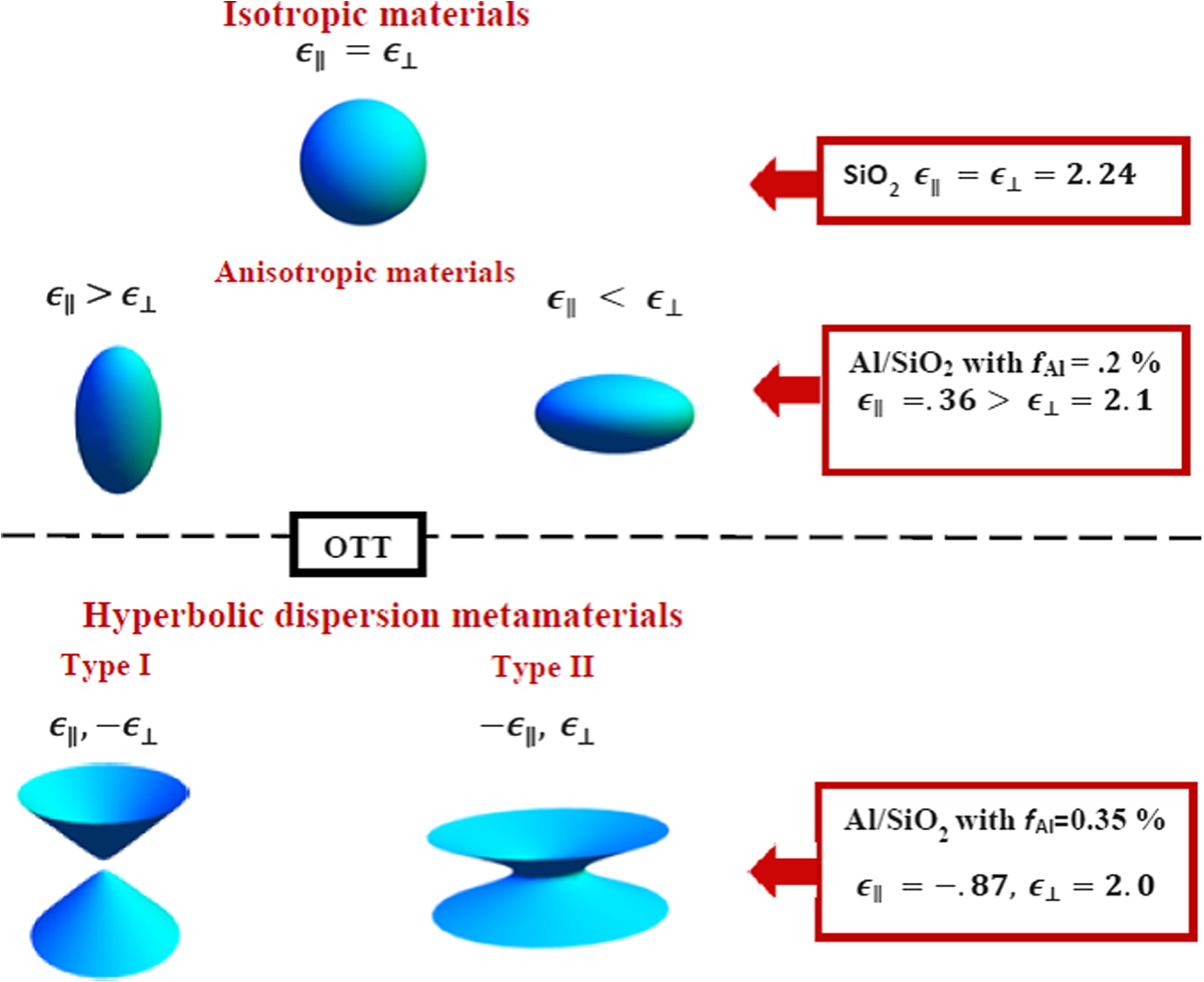 In isotropic materials, e.g., silicon or , reducing the size of the optical cavity (from microcavity to nanocavity) is limited to the fundamental diffraction limit.8 In HMMs, large wavevectors can be achieved along the unbounded IFS. Therefore, optical WGM cavities, created from HMMs, allow the confinement of the electromagnetic field to an extremely small volume,9,10 which opens new opportunities for creating infinitely small three-dimensional (3-D) nanocavities with hyperbolic dispersion and dimensions significantly smaller than the wavelength of light for applications in ultrafast LEDs. In a microcavity, light is emitted into a cavity mode and acquires an enhanced efficiency or emission rate. The Purcell factor ()11 quantifies the enhancement of an atomic emission rate in a cavity versus its rate in free space where is the cavity quality factor, is the resonant wavelength, is the index of refraction of the cavity, and is the effective mode volume given bySuch enhancement is desired for both future quantum information processing and visible light communications. For example, a rate-equation model revealed that when a small (subwavelength) mode volume is combined with a (order of 100), the spontaneous emission rate for an otherwise conventional LED can be enhanced, resulting in a 200-GHz modulation bandwidth.12 Here, we perform finite-difference element numerical simulations for the electromagnetic field confinement and study optical properties of the WGMs in such deep-subwavelength disk nanocavities. This study aims to investigate the fundamental limits for the dimensions of this class of nanocavities, optical mode confinement, and the properties of the nanocavities’ resonance frequencies. The choice of HMMs nanolayered material and silicon substrate material will allow the future incorporation of such nanocavities to the well-established silicon photonics optical communications networks.13 2.Nanolayered Metamaterial Permittivity ModelsWhen designing 3-D nanocavities, the scale of each layer and dispersion of HMM is vital to increasing the bandwidth of such devices, which calls for a detailed model for the dispersion properties of multilayered HMMs. Using aluminum in metal-dielectric structures offers several advantages over these materials. In particular, the plasma frequency of the aluminum is higher than that of gold or silver, which allows for a significant surface plasmon response to occur in the ultraviolet (UV) portion of the spectrum. As a result, aluminum exhibits metallic characteristics over a broader spectral range than gold and silver. In addition, is used as the dielectric for this HMM because it could be easily integrated into current CMOS technology and has near-zero losses in the UV region. In our recent work,14 we used an effective medium approximation (EMA) with nonlocal corrections to describe nanolayered structures with hyperbolic dispersion. Based on our previously published study (Ref. 14), we found that when the Al fill fraction is reduced to 1%, the number of layers does not affect the dielectric function of HMM (for ). In addition, we found that the permittivity of the HMM does not change (Al fraction ) when the thickness of an individual layer is varied from 10 to 2 nm. For the simulations done in this paper, the disk nanocavity is assumed to be made of the nanolayered HMM with 250 nm thickness. The number of the layers () and the thickness of the individual layer () were constant. The nanolayered structure is assumed to be a uniaxial material with different values for the dielectric permittivity in the parallel direction, , and the perpendicular direction, . The permittivity is modeled using EMA.15,16 According to EMA, in-plane permittivity, , and out-of-plane permittivity, , can be described by where is the thickness of aluminum layer ( optical permittivity) and is the thickness of layer ( optical permittivity). The EMA predicts the optical properties of a multilayered structure by combining the known permittivity of the two materials. The optical permittivity for aluminum was obtained by using Drude-critical points model while fitted experimental data from Ref. 17 was used in the infrared region. Silicon dioxide optical permittivity was modeled by using a polynomial fit for experimental data from Ref. 18, which is accurate for spectral range between 300 nm and .Manipulating the Al fill fraction () controls the spectral position of the OTT. The optical permittivity predicted by EMA (Fig. 2) varies with wavelength and fill fraction, which allows for the designing of the material to fit the optical permittivity parameters in desired resonance range. The out-of-plane permittivity, , stays relatively constant while the in-plane permittivity, , varies with small aluminum concentration. The optical permittivity values used for nanocavity studies are chosen near the OTT for a given frequency in an attempt to reduce the effects of the absorption. 3.Computational MethodsCOMSOL’s multiphysics module was used to create a finite element method (FEM) study that produces a resonance frequency and optical mode intensity distribution for the disk nanocavities with different radii. FEM solves a set of weak partial differential Maxwell equations to find the relevant modes.19 The optical mode volume and quality factor were deduced from the intensity distribution. The FEM model is axisymmetric, which is computationally efficient as it allows for symmetric modes to be extrapolated. Over a two-dimensional space, from the edge to the center of the disk, the electric field, electric displacement, and magnetic field were calculated as though they are mirrored around the disk in an azimuthal order () number of times (Fig. 3). Perfectly matched layers, which are not depicted here, were used to simulate infinite space beyond the computation space. Fig. 3(a) , radial electric intensity. (b) Diagram of computation space. The axisymmetric model displays one symmetric node of the resonance. 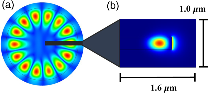 A free triangular mesh was used in the simulation. To ensure triangular mesh properties did not affect the solution, both a Delaunay mesh and a free quadrature mesh were implemented. Changing the mesh type had a minimal effect on the overall simulation (difference ). The smallest mesh settings offered by the COMSOL program are “extra fine” and “extremely fine.” The respective maximum mesh size elements are 32.6 and 16.3 nm. The “extremely fine” mesh was used on disks with radii of 200 nm and lower. Finally, this proved to be adequate as the solutions converged with a tolerance of and retained resolution. While this model allows for exceptional computation times, the axisymmetric nature of this model does not always provide a clear picture of the modes. When reducing mode order to , higher order modes are hard to distinguish from the lowest order mode. FEM models also create spurious mode solutions that solve the required weak form partial differential equations, but have no physical counterpart. These factors must be taken into account for this numerical study. 4.Optical Mode Confinement: Results and DiscussionFirst, the microdisks with various radii (microdisk’s height is 250 nm) were studied using the FEM model (Fig. 4). The free space wavelength of the cavity in Fig. 4 (radius ) is . As the radius decreases, the optical power is leaked around the circumference of the disk. As expected, by , the majority of the optical intensity is outside the cavity and the factor is significantly reduced indicating that the mode is no longer confined within the cavity. Based on the wavelength of the lowest order mode, the diffraction limit for this microdisk optical cavity is around . It indicates (Fig. 4) that no optical mode is likely in microdisks with dimensions smaller than . This result is consistent with previously published experimental and numerical results for silicon microcavities.8 Fig. 4for the lowest order optical mode for the microdisks with different radii . The resonance frequencies are (a) 105.98 THz (), (b) 107.14 THz (), (c) 109.72 THz (), and (d) 111.06 THz (). 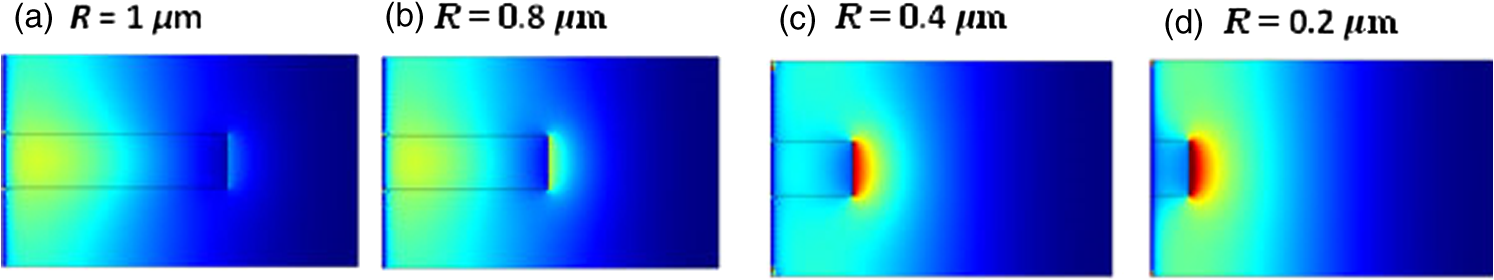 The results of the numerical FEM study for disk nanocavities with different radii (disk nanocavity’s height is 250 nm) show that with hyperbolic dispersion present in the nanolayered material, the optical mode is highly confined in the disk considerably beyond the diffraction limit (Fig. 5). The EMA was used (see Sec. 2) to obtain the dielectric permittivity in the parallel direction, , and in the perpendicular direction, for nanodisks with a different aluminum fill fraction . The wavelength of the optical lower order mode for a disk nanocavity with radius and various aluminum fill fractions was around [Fig. 6(c)]. Figure 5 shows the intensity of the lowest order mode (Al fill fraction is varied between 0.1% and 3.35%) as the radius of the disk is decreased. For all radii, the highest confinement for the optical mode is achieved at the positive side of the OTT with a fill fraction of aluminum between 0.25% and 0.225%. Figure 5 shows that the optical mode is well confined in a disk nanocavity with a radius of up to an order of magnitude smaller than the free-space resonant wavelength . Our recent experimental study20 shows the feasibility of fabrication of the nanolayered films with a low aluminum fill fraction using the RF sputtering technique. Fig. 5for the lowest order optical mode for disk nanocavities with different radii and varying aluminum fill fractions . The optical constants were defined in Sec. 2.  Fig. 6(a) Quality factor and (b) Purcell factor numerically calculated for the lowest optical mode of the disk nanocavities with different radii (between 60 nm and ) and aluminum fill fractions at wavelength . The diffraction limit for nanocavity is indicated by a vertical dotted line (). (c) Real part of the in-plane permittivity () and spectral position of the optical resonant wavelength for nanocavity with radius and various aluminum fill fractions. 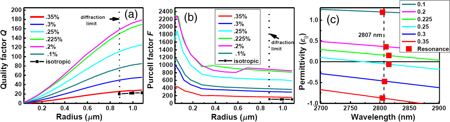 As expected, the -factor diminishes rapidly with decreasing the microdisk’s dimensions [Fig. 6(a)]. In addition, as the fill fraction is increased and the dielectric permittivity in the parallel direction becomes , the -factor is reduced due to presence of higher optical losses for HMMs [Fig. 6(a)]. However, the Purcell factor exhibits a different type of behavior [Fig. 6(b)]. For the lowest order mode (), there is an increase in the Purcell factor for the disk nanocavity. It can be seen that the Purcell factor is an order of magnitude higher for the disk HMM nanocavity compared to the isotropic case ( microdisk) (Fig. 4). Further reducing the nanocavity size () leads to the drop in the factor due to the reducing of the -factor () and, as a result, loss of the optical mode. The disk nanocavity numerical study presented in this paper provides a valuable insight into the enhancement of the optical mode confinement due to hyperbolic dispersion. The strong optical mode confinement results in low radiation loss and, as a result, a higher factor for nanocavities from anisotropic nanolayered metamaterials compared to the nanocavities with isotropic dispersion. Circular disk geometry of a nanocavity results in a lower scattering loss for high- wavevectors compared to the rectangular geometry studied in Ref. 21. The upper bound on the enhancement of the photonic density of states is imposed by the characteristic metamaterial patterning scale.22 Using nanolayered metamaterial with the thickness of the individual layer approaching the atomic layer23 could provide greater flexibility in designing disk nanocavities with highly confined optical modes. Possible incorporation of the laser gain material24 will allow using this type of nanocavity for laser devices and ultrafast LEDs. 5.ConclusionsThe numerical study of the nanocavities with hyperbolic dispersion provides an opportunity to study the unique properties of nanocavities with increased photon density of states and enhanced light–matter interactions. Results of the numerical simulations show that nanocavities with radius of up to an order of magnitude smaller than and Purcell factor reaching are possible to create. Future incorporation of the laser gain material will allow using this type of nanocavity for laser devices and ultrafast LEDs for a variety of applications, from optical communications to biological nanoparticle sensing. AcknowledgmentsThis work was partially supported by the San Diego State University Grant Program (UGP) Award (2015–2016). Priscilla Kelly acknowledges support of a STEM scholarship award funded by the National Science Foundation Grant No. DUE-1259951. ReferencesK. J. Vahala,
“Optical microcavities,”
Nature, 424 839
–846
(2003). http://dx.doi.org/10.1038/nature01939 Google Scholar
Y. Zhang et al.,
“Photonic crystal nanobeam lasers,”
Appl. Phys. Lett., 97 051104
(2010). http://dx.doi.org/10.1063/1.3475397 APPLAB 0003-6951 Google Scholar
B. Ellis et al.,
“Ultralow-threshold electrically pumped quantum dot photonic-crystal nanocavity laser,”
Nat. Photonics, 5 297
–300
(2011). http://dx.doi.org/10.1038/nphoton.2011.51 NPAHBY 1749-4885 Google Scholar
D. R. Smith, J. B. Pendry and M. C. K. Wiltshire,
“Metamaterials and negative refractive index,”
Science, 305
(5685), 788
–792
(2004). http://dx.doi.org/10.1126/science.1096796 SCIEAS 0036-8075 Google Scholar
H. N. S. Krishnamoorthy et al.,
“Topological transitions in metamaterials,”
Science, 336 205
–209
(2012). http://dx.doi.org/10.1126/science.1219171 SCIEAS 0036-8075 Google Scholar
M. Y. Shalaginov et al.,
“Broadband enhancement of spontaneous emission from nitrogen-vacancy centers in nanodiamonds by hyperbolic metamaterials,”
Appl. Phys. Lett., 102 173114
(2013). http://dx.doi.org/10.1063/1.4804262 APPLAB 0003-6951 Google Scholar
D. Lu et al.,
“Enhancing spontaneous emission rates of molecules using nanopatterned multilayer hyperbolic metamaterials,”
Nat. Nanotechnol., 9 48
–53
(2014). http://dx.doi.org/10.1038/nnano.2013.276 NNAABX 1748-3387 Google Scholar
J. Shainline et al.,
“Subwavelength silicon microcavities,”
Opt. Express, 17 23323
–23331
(2009). http://dx.doi.org/10.1364/OE.17.023323 OPEXFF 1094-4087 Google Scholar
X. Yang et al.,
“Experimental realization of three-dimensional indefinite cavities at the nanoscale with anomalous scaling laws,”
Nat. Photonics, 6 450
–454
(2012). http://dx.doi.org/10.1038/nphoton.2012.124 NPAHBY 1749-4885 Google Scholar
C. Bacco, P. Kelly and L. Kuznetsova,
“Optical mode confinement in three-dimensional nano-cavities with hyperbolic dispersion,”
Proc. SPIE, 9544 954419
(2015). http://dx.doi.org/10.1117/12.2187135 PSISDG 0277-786X Google Scholar
E. M. Purcell,
“Spontaneous emission probabilities at radio frequencies,”
Phys. Rev., 69 37
–38
(1946). http://dx.doi.org/10.1103/PhysRev.69.37 PHRVAO 0031-899X Google Scholar
E. K. Lau et al.,
“Enhanced modulation bandwidth of nanocavity light emitting devices,”
Opt. Express, 17 7790
(2009). http://dx.doi.org/10.1364/OE.17.007790 OPEXFF 1094-4087 Google Scholar
Y. Vlasov,
“Applications of integrated photonics technology—from optical interconnects to neurophotonics,”
Advanced Photonics for Communications,
(2014). Google Scholar
P. Kelly, D. White and L. Kuznetsova,
“Theoretical design of nano-layered metamaterial with hyperbolic dispersion with minimum losses,”
Proc. SPIE, 9545 95450B
(2015). http://dx.doi.org/10.1117/12.2187137 PSISDG 0277-786X Google Scholar
L. D. Landau, E. M. Lifshitz and L. P. Pitaevskii, Course of Theoretical Physics, 2nd ed.Reed, Oxford
(1984). Google Scholar
L. M. Brekhovskikh, Waves in Layered Media, 2nd ed.Academic, New York
(1980). Google Scholar
A. Vial and T. Laroche,
“Description of dispersion properties of metals by means of the critical points model and application to the study of resonant structures using the FDTD method,”
J. Phys. D, 40 7152
–7158
(2007). http://dx.doi.org/10.1088/0022-3727/40/22/043 JPAPBE 0022-3727 Google Scholar
R. Kitamura, L. Pilon and M. Jonasz,
“Optical constants of fused quartz from extreme ultraviolet to far infrared at near room temperatures,”
Appl. Opt., 46 8118
–8133
(2007). http://dx.doi.org/10.1364/AO.46.008118 APOPAI 0003-6935 Google Scholar
M. Oxborrow,
“Traceable 2-D finite-element simulation of the whispering-gallery modes of axisymmetric electromagnetic resonators,”
55 1209
–1218
(2007). http://dx.doi.org/10.1109/TMTT.2007.897850 Google Scholar
P. Kelly, A. Martin and L. Kuznetsova,
“Spectroscopic ellipsometry for anisotropic nano-layered metamaterial with hyperbolic dispersion,”
Proc. SPIE, 9919 991909
(2016). http://dx.doi.org/10.1117/12.2237245 PSISDG 0277-786X Google Scholar
J. Yao et al.,
“Three-dimensional nanometer-scale optical cavities of indefinite medium,”
PNAS, 108 11327
–11331
(2011). http://dx.doi.org/10.1073/pnas.1104418108 Google Scholar
Z. Jacob et al.,
“Engineering photonic density of states using metamaterials,”
Appl. Phys. B, 100 215
–218
(2010). http://dx.doi.org/10.1007/s00340-010-4096-5 Google Scholar
P. Kelly, M. Liu and L. Kuznetsova,
“Designing optical metamaterial with hyperbolic dispersion based on an Al:ZnO/ZnO nano-layered structure using the atomic layer deposition technique,”
Appl. Opt., 55 2993
–2997
(2016). http://dx.doi.org/10.1364/AO.55.002993 APOPAI 0003-6935 Google Scholar
J. Smalley et al.,
“Modal amplification in active waveguides with hyperbolic dispersion at telecommunication frequencies,”
Opt. Express, 22 21088
–21105
(2014). http://dx.doi.org/10.1364/OE.22.021088 OPEXFF 1094-4087 Google Scholar
BiographyLyuba Kuznetsova is an assistant professor at the Physics Department at San Diego State University. She received her BS degree in physics from Moscow State University (Moscow, Russia), and her PhD in applied physics from Cornell University in 2008. She is the author of more than 30 journal papers and the coinventor on two patents. Her current research interests include nanophotonics, metamaterials, and lasers. She is a member of OSA and SPIE. |


