
|
|
1.IntroductionHydrogen silsesquioxane (HSQ)1 has been extensively studied as an electron beam (e-beam),2 extreme ultraviolet,3 and imprint lithography4 resist, as well as a low-loss optical cladding for photonic applications.5 Through investigation of the impact of e-beam dose,6,7 development,8–13 and other fabrication parameters14,15 on HSQ surface roughness and contrast, lines as narrow as 4.5 nm have been demonstrated.16 Resist line edge roughness (LER) and the related line width roughness are key fabrication parameters for a variety of structures found in electronics,17 photonics,18–21 and microelectromechanical systems.22 The dominant source of LER in e-beam resists is the lightly dosed polymer aggregates that form at the edge of exposed resist patterns.6,23–26 During pattern transfer, mask LER creates sidewall roughness (SWR) which is the dominant propagation loss mechanism in silicon waveguides. HSQ is a promising resist for reduced LER due to its three-dimensional (3-D) network structure and low molecular weight.2 Optical transmission losses in Si waveguides have been reported for both shallowly etched rib waveguides27 and waveguides with fabrication based on thermal oxidation.28–30 Both of these low-loss designs exchange reduced loss for increased mode size and required chip area. In contrast, fully etched silicon strip waveguides exhibit single-mode operation with submicrometer rectangular cross sections and enable compact integrated optical circuits.31 Low-loss strip waveguides are required for geometries such as slot32,33 and nanobeam34 waveguides. Although several authors have previously reported fully etched waveguides with losses ,35–38 a comprehensive multiparameter study on optimizing HSQ mask LER to achieve low-loss strip waveguides including both fabrication and optical characterization has not been reported. In this work, we present the results of a study on the influence of pre-exposure and postexposure baking, e-beam spot size and dosing, and multipass writing techniques on HSQ mask LER and demonstrate a significant reduction in the optical propagation losses of the fabricated waveguides with the optimized fabrication parameters. Mask LER is reduced for oven pre-exposure baking at 50°C, high exposure doses with beam spot sizes larger than the e-beam step size (BSS), development in high contrast 25% tetramethylammonium hydroxide (TMAH, J.T. Baker), and postdevelopment baking with rapid thermal annealing (RTA) in an ambient. Further reduction in LER is demonstrated using multipass writing with intentional offsets applied for each e-beam write pass. Direct 3-D atomic force microscopy (3-D AFM) measurements of the SWR show average root-mean-square (RMS) roughness of 2.1 nm and correlation length of 94 nm. Optical propagation loss measurements are used to confirm the reduction in SWR once the optimized fabrication parameters are established. Fully etched Si waveguides, patterned with low-LER HSQ masks, with 450-nm widths and 250-nm heights are measured to have average losses for both transverse electric (TE) and transverse magnetic (TM) modes across the telecommunications C-band (1530 to 1565 nm). A comparison of TE-mode losses from a previous work39 fabricated without the reduced LER HSQ mask shows an improvement of for the best results reported here. This paper is organized as follows. Section 2 describes the experimental parameter space studied in this work along with the measurement techniques used to characterize test structures. Section 3 details the results of our multiparameter study on HSQ mask LER. Section 4 discusses the results and compares the simulated and measured optical losses due to SWR. Concluding remarks are given in Sec. 5. 2.Experimental2.1.Spin Coating and Pre-Exposure Bake ParametersHSQ thin films are obtained by spin coating 4% HSQ (Dow-Corning XP1541-4) in methyl isobutyl ketone onto Si substrates and silicon on insulator (SOI, Soitec) substrates with a top Si thickness of 250 nm and buried oxide (BOX) thickness of 1 μm. Si substrate samples are used to study the effects of fabrication parameters on HSQ mask LER, while SOI samples are used for optical propagation loss measurements. Comparisons of the etch profiles of Si and SOI samples show no discernible difference in dimensions or SWR. Spin coating the samples at 3000 rpm results in approximately 80 nm of HSQ. Immediately after spin coating, samples are baked for 40 min in a purged oven at temperatures ranging from 50 to 200°C. Additional samples are baked for 40 min at room temperature in a YES III HMDS Vapor Prime/Vacuum Oven. After pre-exposure baking, samples are loaded into a Vistec EBPG 5000 e-beam lithography tool for patterning at 100 kV acceleration voltage. 2.2.E-Beam Writing Parameters and DevelopmentExposed patterns consist of straight lines, rings with bus waveguides, and tapered width sections. Lines and rings have a designed width of 450 nm. Rings with bus waveguides have coupling gaps between 100 and 500 nm. Tapered width sections vary in width from 60 to 450 nm. We create ring resonator waveguides with radii from 2.5 to 10 μm as a series of 0.5 deg arc segments for 30 deg on either side of the bus coupling section and 1 deg arc segments elsewhere. The e-beam current, dose, and BSS are related by , where is the current in nA, is the beam sweep frequency in MHz, is the per-pass dose in and BSS is the beam step size in μm. To minimize writing time, the beam sweep frequency is fixed at the machine maximum value of 10 MHz. Similarly, in order to better reproduce curved mask geometries with the rectangular and trapezoidal subsections into which the digital mask file is fractured for e-beam writing, the BSS is fixed at the machine minimum of 5 nm. With these values fixed, there is a linear relationship between the beam current and per-pass dose. In addition, the beam spot size is linked to the beam current. For currents in the range of 625 pA to 3.125 nA, the beam spot size (diameter) varies from 5 to 11 nm, as theoretically determined by the e-beam vendor. Patterns are written using four-pass writing. In this writing scheme, the beam is scanned over the same region four times, delivering a quarter of the total dose in each pass, before moving to the next writefield. Intentional per-pass offsets are implemented by shifting the pattern file by one BSS between each pass.40 Curved structures are rotationally offset by a fraction of the minimum prefractured arc segment length used to make up the curved regions. For ring resonators with 0.5 deg arc segments and four-pass writing with per-pass offsets, each pass used to expose the HSQ is then rotated by 0.125 deg from the previous. Exposed samples are developed in TMAH. The contrast of TMAH-based HSQ development can be increased through several factors including increasing developer concentration,7 increasing developer temperature,9,10 and by adding salts to the development solution.11,12,16 Since hot TMAH acts as an effective Si etchant,10,41 we focus only on the role of developer concentration on the HSQ mask LER. All development is carried out at 25°C. Careful control of development temperature is critical since variations as small as 1°C have been reported to result in significant changes in contrast and onset dose.9 Top-side HSQ surface roughness is characterized with an Asylum MFP-3-D AFM. 2.3.Postdevelopment ProcessingAfter development, samples are hard-baked either on a 350°C hotplate for 2 min, or on a 150°C hotplate for 2 min followed by a 1000°C anneal in an ambient for 1 min in an AGA 410 RTA. The 150°C hotplate bake is used before inserting the samples into the RTA to drive off any remaining solvent and prevent RTA chamber contamination. Si etching is performed in a PlasmaTherm SLR770 Inductively Coupled Plasma-Reactive Ion Etcher (ICP-RIE) with chemistry. For this work, etching conditions are kept constant for all samples in order to isolate the role of the mask LER on the waveguide profile. The HSQ mask is not removed from the samples after etching since it forms a low-loss optical cladding after hardbake.5 Half of the samples used for optical propagation loss measurements are treated with a postetch bake at 1000°C in RTA in an ambient for 1 min immediately following etching. We primarily characterize the impact of fabrication parameters through qualitative scanning electron microscope (SEM) analysis of both top-down and cross-sectional images of etched Si patterns on Si substrates using a Zeiss Ultra 55 Plus FE-SEM. Given the established fabrication parameters based on SEM analysis, optical propagation loss measurements are used to confirm the reduced waveguide SWR. SOI samples used for optical transmission loss measurements are clad with 1 μm plasma enhanced chemical vapor deposition (PECVD) in a PlasmaTherm 790 PECVD tool using a chemistry. Finally, compact cantilever couplers are fabricated to allow low-loss fiber-to-chip coupling for optical characterization.39 2.4.Characterization of Etched WaveguidesAlthough qualitative SEM analysis is a useful tool for rapid prototyping and analysis of recipe parameters, it does not give quantitative information about LER or SWR. Direct quantitative measurement of SWR with conventional techniques such as top-down AFM and SEM is challenging. 3-D AFM is a relatively new technique that allows for direct, nondestructive characterization of the sidewalls of submicron structures.42–46 Since propagation losses in fully etched silicon strip waveguides are sensitive to variations in SWR that are small compared to the total feature size,31 accurate nondestructive analysis with 3-D AFM is a promising technique for the study and optimization of fabrication processes. Optimized waveguide SWR is characterized both directly through 3-D AFM and indirectly though optical propagation loss measurements. 3-D AFM measurements are performed with a Park Systems NX-3DM which tilts the sample stage by to directly measure the sidewalls of the 250-nm tall Si waveguides with a standard high aspect ratio AFM tip.45,46 The NX-3DM system has a resolution of and a noise level of . Optical propagation losses are determined through both resonant and nonresonant techniques. Straight waveguide propagation losses are calculated by measuring the total fiber-to-fiber insertion loss for waveguides with lengths ranging from 1 mm to 2 cm. By fitting a line to the increasing loss with waveguide length, propagation losses are calculated by the slope and total coupling losses are calculated from the abscissa intercept. Once fiber-to-chip coupling is established, measured power is stable with fluctuations in power. Based on this measurement uncertainty, propagation losses fit from multiple waveguide measurements are conservatively estimated to be . All waveguides with lengths greater than 5 mm include four 30-μm radius 90 deg bends to confirm that light is guided in the Si waveguide rather than in the oxide slab. Losses in ring resonators are determined from critically coupled single-bus rings and from dual-coupled rings. Both the coupling between the bus and ring waveguides and the loss inside the resonator influence the ring resonator transmission response.47 3.Results3.1.Pre-Exposure BakeAs the pre-exposure bake temperature is increased from 50 to 200°C, the measured top-side RMS roughness of samples exposed and developed in 2.38% TMAH (Rohm and Haas, MF-CD-26) tends to increase for all tested doses. Samples baked at 50°C have a maximum top-side roughness of 3.1 nm for lower doses () and 1.0 nm for higher doses (). Samples baked at 200°C show roughness values as large as 7.7 nm for lower doses and similarly low roughness of 1.3 nm for higher doses. Samples baked at the intermediate temperatures of 100 and 150°C show a similar decrease in top-side roughness from 3.6 to 1.2 nm and from 3.1 to 1.2 nm, respectively, over the same range of exposure doses. Since using a 50°C pre-exposure bake reduces the maximum top-side roughness for lightly dosed resist and the LER of fully dosed resist is comparable to the top-side roughness of lightly dosed resist,23 low temperature pre-exposure baking results in minimized LER. Trends in HSQ roughness with exposure dose are expected to be similar for both low and high contrast TMAH development for samples with the same pre-exposure bake temperature.7 Pre-exposure bake temperatures lower than 50°C were not further explored since uneven lines were observed on these samples during postetch inspection. 3.2.E-Beam Writing Parameters and DevelopmentWe observe a clear trend in reduced HSQ mask LER with an increased exposure dose from 320 to and the corresponding increase in beam current from 200 pA to 3.125 nA and spot size from 4 to 11 nm. As the dose and beam spot size increase, dimensions of developed patterns tend to increase laterally and thin resist residues form between closely spaced patterns, as shown in the nominally 100 nm gaps in Figs. 1(a) and 1(b). By switching from a low contrast developer, 2.38% TMAH, to a high contrast developer, 25% TMAH, properly sized patterns with clean gaps are produced as shown in Figs. 1(c) and 1(d). Figure 2 provides comparative SEM micrographs showing the impact of increased dose and beam current on waveguide LER. The minimum dose required to produce viable waveguide patterns increases from approximately for 2.38% TMAH to approximately for 25% TMAH. For either developer, increasing the total dose to at least three times larger than this minimum value results in a significant decrease of LER. The optimal HSQ LER for samples with a 50°C pre-exposure bake corresponds to a total dose of with an approximately 11-nm beam spot size and development in 25% TMAH. Fig. 1Scanning electron microscopy (SEM) images showing the result of developer concentration and beam writing techniques on etched Si patterns on Si substrate: (a) and (b) bus and ring waveguides written with a dose and developed with low-contrast 2.38% tetramethylammonium hydroxide (TMAH) without and with 0.125 deg per-pass rotational offset, respectively; (c) and (d) bus and ring waveguides written with a dose and developed with high-contrast 25% TMAH without and with 0.125 deg per-pass rotational offset in the ring section, respectively. The fabrication process for all four samples includes a 50°C pre-exposure bake and postexposure bake for 1 min at 1000°C in a rapid thermal annealing (RTA) in an ambient. All images are at the same scale and the hydrogen silsesquioxane (HSQ) mask is intact. 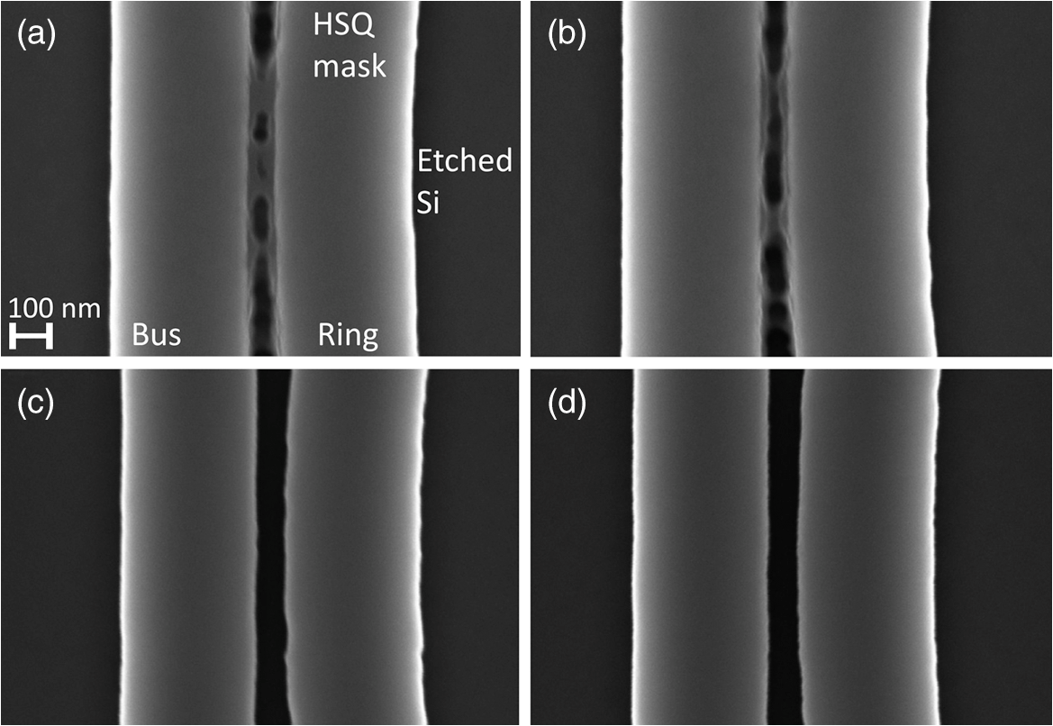 Fig. 2Top-down SEM images of etched Si demonstrating the impact of exposure dose on mask line edge roughness: (a) exposure dose, 0.625 nA beam current, and 5.2 nm spot size; (b) exposure dose, 1.25 nA beam current, and 6.7 nm spot size; (c) exposure dose, 1.875 nA beam current, and 8.0 nm spot size. The beam current is changed along with the dose to maintain the beam sweep frequency near 10 MHz. The fabrication process for all three samples includes 50°C pre-exposure bake, four-pass writing with per-pass offsets, development in 2.38% TMAH, and postexposure bake for 1 min at 1000°C in an RTA in an ambient. All images are at the same scale and the HSQ mask is intact. 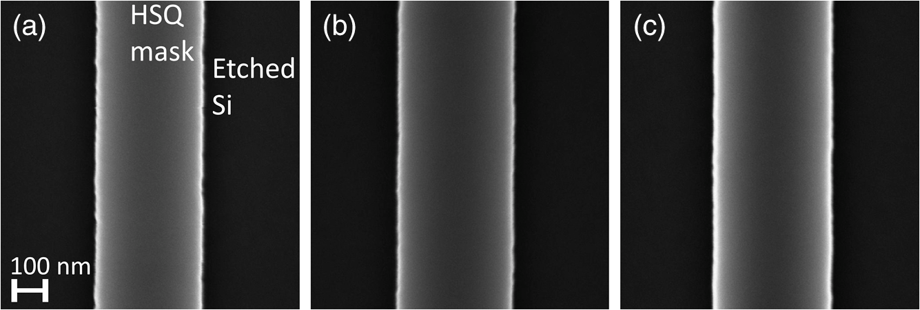 Next, we studied the impact of per-pass pattern shifting on both straight and curved structures. For straight structures, the effect of per-pass offsets is mainly to minimize the impact of mechanical vibrational noise and stitches between writefields. Based on SEM analysis, stitch error is reduced for four-pass writing where each pass is shifted by one BSS away from the designed position in each coordinate direction (, ). Top-down SEM micrographs of bus-coupled ring waveguides without, Figs. 1(a) and 1(c), and with, Figs. 1(b) and 1(d), per-pass rotational offset are given in Fig. 1. The LER visible on the left edge of the ring structure in Fig. 1(c) has been smoothed out due to per-pass rotational offsets in the corresponding region of Fig. 1(d). The LER of the straight bus waveguides in Figs. 1(c) and 1(d) is similar since rotational offsets are not used for straight structures. 3.3.Postdevelopment BakeWe next explored the impact of hardbake conditions on mask LER. Cross-sectional SEM micrographs of etched Si samples hotplate baked at 350°C show significantly more roughness than those RTA baked at 1000°C in an ambient, as presented in Fig. 3. Annealing HSQ in an ambient breaks remaining Si-H bonds and densifies the film to form a low-loss optical cladding.5 By annealing before etching, the increased density also improves the ICP-RIE etch selectivity. For our etch chemistry, Si:mask selectivity increases from with hotplate baking to for the RTA process. The increased Si:mask selectivity for samples baked in RTA, Figs. 3(b) and 3(c), results in a thicker HSQ layer after etching compared to hotplate baked samples, Fig. 3(a). During annealing, the HSQ films shrink by approximately 21% in the vertical direction. By comparison, the widths of the HSQ films shrink by approximately 5 nm or of the designed 450 nm width. Masking from that forms during RTA causes the reduced etch depth shown in Figs. 3(b) and 3(c). Fig. 3Angled cross-sectional SEM images of etched Si showing the result of postdevelopment baking on the SWR and etching uniformity: (a) 350°C hot plate bake for 2 min; (b) and (c) 1000°C RTA bake in ambient for 1 and 2 min, respectively. The fabrication process for all three samples includes a 50°C pre-exposure bake, total exposure dose with four-pass writing, and development in 2.38% TMAH. All images are at the same scale and the HSQ mask is intact. 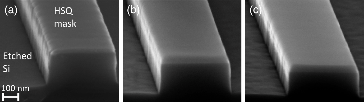 Top-down and angled cross-sectional SEM micrographs of etched Si patterned with the optimal parameters found in this study are given in Figs. 4(a) and 4(b), respectively. LER is visible in the top-down image. The striations on the sidewall of Fig. 4(b) correspond to pattern width variations from LER in the HSQ mask. A summary of the fabrication parameters studied and the corresponding optimized recipe values is given in Table 1. Optimized process parameters are 50°C pre-exposure bake, total exposure dose with a 3.125 nA beam and 11-nm beam spot size, four-pass writing with per-pass linear and rotational offsets, development in 25% TMAH, and postexposure baking at 1000°C in RTA in an ambient. Fig. 4SEM images of etched Si produced with optimized HSQ mask: (a) top-down and (b) angled cross sectional. Both images show Si patterns on a Si substrate with the HSQ mask intact. 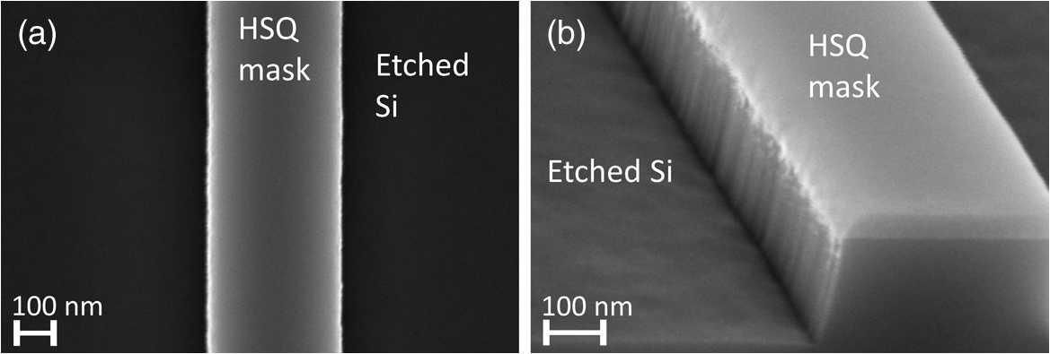 Table 1Summary of the multiparameter fabrication study and the optimized values for each parameter.
3.4.Sidewall RoughnessFigure 5(a) shows a 3-D AFM image of etched Si after the HSQ mask has been removed with hydrofluoric acid etching. The SWR in Fig. 5(a) corresponds to the striations of Fig. 4(b). Six total fine scans with a 9-μm length and a 9.7 nm step size are measured along both sidewalls of straight structures at heights of 40, 100, and 160 nm from the Si surface. A 3-D AFM profile scan taken at a height of 100 nm is shown in Fig. 5(b). Except for the abrupt transition seen at approximately 1.5 μm, the scan shows a relatively smooth sidewall variation that stays within of ideal for the remaining 7.5 μm. All scans show similar roughness profiles from the top to the bottom of the waveguide sidewall, indicating that the LER of the mask is directly transferred into SWR through anisotropic etching. The measured RMS roughness, averaged from the six fine line scans, is 2.1 nm. The correlation length of the roughness is determined by fitting an exponential to the autocorrelation function of the 3-D AFM profile data, as shown in Fig. 6.31 The spatial autocorrelation function measures the similarity of the roughness profile with a copy shifted by the lag length. The extracted correlation length is 94 nm, averaged across all line scans. The oscillations in the autocorrelation function originate from oscillations in the measured waveguide width in the roughness scan, Fig. 5(b), with the same period. Both the RMS roughness and the roughness correlation length are required for theoretical or simulated estimation of waveguide propagation loss.31 Fig. 5(a) 3-D AFM image of etched straight waveguide section with the HSQ mask removed. 3-D AFM measurements are performed on etched Si patterns on Si substrate. (b) Measurement of the sidewall position measured by 3-D AFM. The sidewall profile has been normalized to pass along but not smoothed.  Fig. 6Plot of the autocorrelation function for the 3-D AFM scan of the straight waveguide sidewall given in Fig. 5(b). An exponential fit to the autocorrelation result gives a roughness correlation length of 97.7 nm. The measured RMS roughness for this scan is 1.8 nm.  3.5.Transmission LossA variety of test structures are used to characterize the optical propagation losses of waveguides fabricated with optimized HSQ masks. An etched Si dual-coupled ring resonator structure similar to those used for resonant measurement of propagation losses is shown in Fig. 7. The ring resonator exhibits minimal LER and nominally equal coupling gaps to the two bus waveguides. Figure 8 presents the measured ring resonator spectra for single-bus coupled and dual-bus coupled rings. TM-mode single-bus ring resonators near their critical coupling gaps demonstrate quality factors as high as 122,000. Optical propagation losses calculated from critically coupled single-bus rings and dual-coupled through- and drop-port transmission measurements of dual-bus rings like those shown in Fig. 7 give values of 3.6 to . Extracted propagation losses based on straight waveguide measurements are given in Fig. 9(a). When averaged across the telecommunications C-band, TE-mode propagation losses are 2.4 and for waveguides with and without the additional postetch RTA, respectively. TM-mode propagation losses are both with and without the additional postetch RTA bake. Measured losses for ring waveguides are larger than those for straight waveguides due to both increased roughness in curved structures and larger measurement error in determining the loss in resonant structures. Error sources in resonant measurements include uncertainty of the critical coupling condition for single-bus coupled rings and differences in the coupling coefficients between the ring and two bus waveguides for dual-bus coupled rings.47 Table 2 provides a summary of the 3-D AFM SWR and optical propagation loss measurements. Fiber-to-chip coupling losses averaged across the C-band for all samples are . Fig. 7SEM images of etched Si waveguides on Si substrate. (a) Top-down view showing dual-bus and single-bus coupled ring resonator patterns. (b) Close-up view of the dual-bus coupled ring resonator shown in the dashed box in (a).  Fig. 8Measured ring resonator spectra for 10-μm radius TM-mode ring resonator waveguides: (a) Single-bus coupled ring with a quality factor of 113,000. (b) Dual-bus coupled ring response used for estimating curved waveguide propagation losses without the requirement for critical coupling. The extracted propagation loss in this ring is as determined by the symmetric coupled ring method (Ref. 47).  Fig. 9Measured optical propagation losses of SOI waveguides: (a) average TE-mode and TM-mode losses are 2.8 and across the telecommunications C-band, respectively. (b) Comparison of TE-mode losses with the optimized HSQ mask to waveguides fabricated without the optimizations reported in this work. 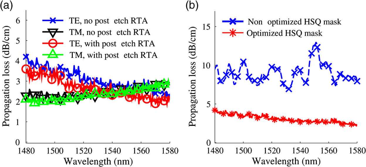 Table 2Summary of 3-D AFM SWR and optical propagation loss measurement results. Propagation losses are not given for TE-mode ring resonators due to the observation of split resonances.
4.DiscussionThroughout this multiparameter study on the impact of HSQ mask LER on the etch profile of Si waveguides, we focus on techniques to create a mask with reduced size polymer aggregates. As an example, the optimal pre-exposure bake temperature of 50°C corresponds to the lowest viable temperature tested and the smallest amount of pre-exposure HSQ crosslinking.15 Since pre-exposure linking is minimized, we expect that lightly dosed HSQ outside of the patterned regions will be more likely to be developed away, especially with high contrast 25% TMAH. By increasing the e-beam current such that the beam spot size is more than twice as large as the BSS, we increase the overlap between adjacent e-beam shots which results in a more uniform resist edge exposure profile. The basic four-pass ring resonator pattern file without per-pass offsets consists of 480 arc segments with 960 unique vertices. When four-pass writing with per-pass rotational offsets is used, the number of unique vertices increases to 3840. This increase in vertex count again results in additional exposure overlap and minimizes the formation of sharp corners formed at the pattern edges and isolated vertices generated during fracturing. Although the number of vertices could be further increased by using additional exposure passes with smaller rotations, this would come at the expense of reduced per-pass dose which results in a smaller beam spot size and longer e-beam writing time. Increasing HSQ process contrast has been the focus of many prior studies8–11,13,15 with the goal of producing narrow HSQ patterns. In this work, increased contrast with higher developer concentration allows for the use of beam spot sizes larger than the BSS without sacrificing clean sub-100 nm gaps required in many Si photonics applications.32–34 We attribute much of the reduction in LER to increased dose, high development contrast, and the use of RTA in for postdevelopment baking. During the mask hardbake, the HSQ mask transforms into a dense network structure and begins to reflow.48,49 The increased etch selectivity that also comes from the RTA step allows for the thinner initial HSQ films required for high resolution structures50 or for high aspect-ratio waveguides. The use of a second, postetch RTA bake in ambient further reduces TE-mode propagation losses by while having little impact on TM-mode losses. The disparity suggests that the second anneal step primarily functions to grow a thin thermal oxide on the waveguide sidewalls where the TE-mode is more strongly localized. The combination of reduced propagation losses and low-loss coupling from the compact cantilever couplers results in a total fiber-to-fiber insertion loss of for a 1-cm long waveguide in either TE-mode or TM-mode. The loss spectra in Fig. 9(a) for TE-mode and TM-mode exhibit opposite trends with increasing wavelength due to the multiple dominant loss sources including sidewall scattering and substrate leakage which contribute to the total waveguide propagation loss. For wavelengths far from cutoff, propagation losses due to SWR for both modes decrease with increasing wavelength as the size of the SWR decreases relative to the wavelength.51 The increasing loss with wavelength for the TM-mode is explained by increasing the substrate leakage through the 1 μm BOX layer as the optical mode is less confined inside the Si core. Comparing the propagation losses in Fig. 9(b) of waveguides optimized in this study to those of our earlier work,39 we observe a significant reduction not only in the propagation losses but also in the amplitude of ripple in loss spectra. Average TE-mode losses across the telecommunications C-band are reduced from 9.4 to by improving the HSQ mask LER. The spectral ripple shown in Fig. 9(b) arises from the net effect of multiple waveguides, each with its own spectral response, that are used to extract the propagation losses. The total insertion loss, including both fiber-to-chip coupling and propagation losses, for several waveguides with lengths ranging from 0.3 to 2 cm is given in Fig. 10. The spectral response of an individual waveguide is caused by SWR which contributes both to radiation and backscattering.52 By reducing the waveguide SWR, spectral ripple is also reduced. Fig. 10Measured total optical fiber-to-fiber insertion loss for TM-mode propagation through waveguides with lengths from 0.3 to 2 cm. The ripples in the spectral response differ for each waveguide due to the variations in sidewall roughness (SWR) for each measured device. Insertion loss for shorter waveguides is dominated by fiber-to-chip coupling which is relatively insensitive to wavelength (Ref. 39). For longer waveguide lengths, the insertion loss is increasingly due to the propagation and, therefore, shows a stronger dependence on the wavelength. 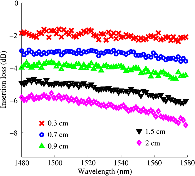 Finally, full 3-D finite difference time domain (Lumerical FDTD Solutions, Vancouver, Canada) simulations are used to compare the Si waveguide SWR as measured directly with 3-D AFM and indirectly through optical propagation loss. Propagation loss due to SWR is simulated by varying the waveguide width along a 200-μm long waveguide to match a given RMS roughness, correlation length, and roughness profile. Simulations of a Si strip waveguide with 450-nm width, 250-nm height, RMS SWR of 2.1 nm, and an exponential roughness profile with a correlation length of 94 nm result in TE-mode and TM-mode simulated losses of 4.4 and , respectively, averaged from 1530 to 1565 nm. Simulated and measured losses show relatively good agreement. 5.Summary and ConclusionsWe have studied the impact of HSQ e-beam fabrication parameters on mask LER and the SWR it generates on etched Si waveguides. Improved LER is achieved through 50°C pre-exposure baking, four-pass exposure with total dose and a beam spot size more than twice as large as the e-beam BSS, development in 25% TMAH and postdevelopment baking in an RTA in an ambient at 1000°C. For curved structures, we observe reduced LER and errors due to pattern fracturing with per-pass rotational offsets compared to samples without per-pass rotational offsets. 3-D AFM measurements of etched sidewalls show an RMS roughness of 2.1 nm with a correlation length of 94 nm. Optical propagation losses of these 450-nm wide by 250-nm tall waveguides are and for TM- and TE-mode light, respectively, averaged over the telecommunications C-band. Additional loss reduction for the TE-mode light is observed for postetch baking in an RTA at 1000°C in an ambient. Further reduction in optical propagation losses would be possible through the use of an e-beam tool with a smaller minimum BSS which would further reduce pattern digitization errors and improve resist exposure uniformity. AcknowledgmentsWe thank David Sampson, Harry Cho, and Louis Han of Park Systems Corp. for 3-D AFM measurements. We also thank Qiang Xu for assistance with FDTD simulations. The authors acknowledge support from the National Science Foundation Award 0954996 and the Air Force Research Laboratory Contract FA8650-09-C-1619. M.W., J.B., and R.R. designed the multiparameter study. M.W., L.C., and J.B. fabricated and characterized the Si test samples. M.W. and L.C. measured optical propagation losses. R.R. supervised all aspects of the work. ReferencesC. L. FryeW. T. Collins,
“The oligomeric silsesquioxanes, ,”
J. Am. Chem. Soc., 92
(19), 5586
–5588
(1970). http://dx.doi.org/10.1021/ja00722a009 JACSAT 0002-7863 Google Scholar
H. Namatsuet al.,
“Three-dimensional siloxane resist for the formation of nanopatterns with minimum linewidth fluctuations,”
J. Vac. Sci. Technol. B, 16
(1), 69
–76
(1998). http://dx.doi.org/10.1116/1.589837 JVTBD9 0734-211X Google Scholar
Y. Ekinciet al.,
“20 nm line/space patterns in HSQ fabricated by EUV interference lithography,”
Microelectron. Eng., 84
(5–8), 700
–704
(2007). http://dx.doi.org/10.1016/j.mee.2007.01.213 MIENEF 0167-9317 Google Scholar
D. P. Manciniet al.,
“Hydrogen silsesquioxane for direct electron-beam patterning of step and flash imprint lithography templates,”
J. Vac. Sci. Technol. B, 20
(6), 2896
–2901
(2002). http://dx.doi.org/10.1116/1.1515311 JVTBD9 0734-211X Google Scholar
C. W. HolzwarthT. BarwiczH. I. Smith,
“Optimization of hydrogen silsesquioxane for photonic applications,”
J. Vac. Sci. Technol. B, 25
(6), 2658
–2661
(2007). http://dx.doi.org/10.1116/1.2787832 JVTBD9 0734-211X Google Scholar
H. Namatsuet al.,
“Influence of edge roughness in resist patterns on etched patterns,”
J. Vac. Sci. Technol. B, 16
(6), 3315
–3321
(1998). http://dx.doi.org/10.1116/1.590375 JVTBD9 0734-211X Google Scholar
Y. M. Georgievet al.,
“Surface roughness of hydrogen silsesquioxane as a negative tone electron beam resist,”
Vacuum, 77
(2), 117
–123
(2005). http://dx.doi.org/10.1016/j.vacuum.2004.07.080 VACUAV 0042-207X Google Scholar
W. HenschelY. M. GeorgievH. Kurz,
“Study of a high contrast process for hydrogen silsesquioxane as a negative tone electron beam resist,”
J. Vac. Sci. Technol. B, 21
(5), 2018
–2025
(2003). http://dx.doi.org/10.1116/1.1603284 JVTBD9 0734-211X Google Scholar
Y. ChenH. YangZ. Cui,
“Effects of developing conditions on the contrast and sensitivity of hydrogen silsesquioxane,”
Microelectron. Eng., 83
(4–9), 1119
–1123
(2006). http://dx.doi.org/10.1016/j.mee.2006.01.167 MIENEF 0167-9317 Google Scholar
S. Choiet al.,
“Effects of developer temperature on electron-beam-exposed hydrogen silsesquioxane resist for ultradense silicon nanowire fabrication,”
J. Vac. Sci. Technol. B, 25
(6), 2085
–2088
(2007). http://dx.doi.org/10.1116/1.2794315 JVTBD9 0734-211X Google Scholar
J. K. W. YangK. K. Berggren,
“Using high-contrast salty development of hydrogen silsesquioxane for sub-10-nm half-pitch lithography,”
J. Vac. Sci. Technol. B, 25
(6), 2025
–2029
(2007). http://dx.doi.org/10.1116/1.2801881 JVTBD9 0734-211X Google Scholar
J. Kimet al.,
“Understanding the base development mechanism of hydrogen silsesquioxane,”
J. Vac. Sci. Technol. B, 27
(6), 2628
–2634
(2009). http://dx.doi.org/10.1116/1.3250261 JVTBD9 0734-211X Google Scholar
H.-S. Leeet al.,
“Two-step resist-development process of hydrogen silsesquioxane for high-density electron-beam nanopatterning,”
J. Vac. Sci. Technol. B, 27
(1), 188
–192
(2009). http://dx.doi.org/10.1116/1.3049482 JVTBD9 0734-211X Google Scholar
D. Küpperet al.,
“Impact of supercritical drying on roughness of hydrogen silsesquioxane e-beam resist,”
J. Vac. Sci. Technol. B, 24
(2), 570
–574
(2006). http://dx.doi.org/10.1116/1.2167990 JVTBD9 0734-211X Google Scholar
M. Häffneret al.,
“Influence of temperature on HSQ electron-beam lithography,”
J. Vac. Sci. Technol. B, 25
(6), 2045
–2048
(2007). http://dx.doi.org/10.1116/1.2794324 JVTBD9 0734-211X Google Scholar
J. K. W. Yanget al.,
“Understanding of hydrogen silsesquioxane electron resist for sub-5-nm-half-pitch lithography,”
J. Vac. Sci. Technol. B, 27
(6), 2622
–2627
(2009). http://dx.doi.org/10.1116/1.3253652 JVTBD9 0734-211X Google Scholar
W. Steinhöglet al.,
“Impact of line edge roughness on the resistivity of nanometer-scale interconnects,”
Microelectron. Eng., 76
(1–4), 126
–130
(2004). http://dx.doi.org/10.1016/j.mee.2004.07.005 MIENEF 0167-9317 Google Scholar
K. K. Leeet al.,
“Effect of size and roughness on light transmission in a waveguide: experiments and model,”
Appl. Phys. Lett., 77
(11), 1617
–1619
(2000). http://dx.doi.org/10.1063/1.1308532 APPLAB 0003-6951 Google Scholar
F. Grillotet al.,
“Size influence on the propagation loss induced by sidewall roughness in ultrasmall SOI waveguides,”
IEEE Photonic. Technol. Lett., 16
(7), 1661
–1663
(2004). http://dx.doi.org/10.1109/LPT.2004.828497 IPTLEL 1041-1135 Google Scholar
S. Sardoet al.,
“Line edge roughness (LER) reduction strategy for SOI waveguides fabrication,”
Microelectron. Eng., 85
(5–6), 1210
–1213
(2008). http://dx.doi.org/10.1016/j.mee.2008.01.035 MIENEF 0167-9317 Google Scholar
D. Lauvernieret al.,
“Optimization of HSQ resist e-beam processing technique on GaAs material,”
Microelectron. Eng., 75
(2), 177
–182
(2004). http://dx.doi.org/10.1016/j.mee.2004.05.002 MIENEF 0167-9317 Google Scholar
M. A. Mohammadet al.,
“Fabrication of sub-10 nm silicon carbon nitride resonators using a hydrogen silsesquioxane mask patterned by electron beam lithography,”
Microelectron. Eng., 88
(8), 2338
–2341
(2011). http://dx.doi.org/10.1016/j.mee.2010.11.045 MIENEF 0167-9317 Google Scholar
M. Nagaseet al.,
“Nano-scale fluctuations in electron beam resist pattern evaluated by atomic force microscopy,”
Microelectron. Eng., 30
(1–4), 419
–422
(1996). http://dx.doi.org/10.1016/0167-9317(95)00277-4 MIENEF 0167-9317 Google Scholar
T. Yamaguchiet al.,
“Nanometer-scale linewidth fluctuations caused by polymer aggregates in resist films,”
Appl. Phys. Lett., 71
(16), 2388
–2390
(1997). http://dx.doi.org/10.1063/1.120037 APPLAB 0003-6951 Google Scholar
H. Namatsuet al.,
“Nano-patterning of a hydrogen silsesquioxane resist with reduced linewidth fluctuations,”
Microelectron. Eng., 41/42 331
–334
(1998). http://dx.doi.org/10.1016/S0167-9317(98)00076-8 MIENEF 0167-9317 Google Scholar
E. Gogolideset al.,
“A review of line edge roughness and surface nanotexture resulting from patterning processes,”
Microelectron. Eng., 83
(4–9), 1067
–1072
(2006). http://dx.doi.org/10.1016/j.mee.2006.01.162 MIENEF 0167-9317 Google Scholar
P. Donget al.,
“Low loss shallow-ridge silicon waveguides,”
Opt. Express, 18
(14), 14474
–14479
(2010). http://dx.doi.org/10.1364/OE.18.014474 OPEXFF 1094-4087 Google Scholar
K. K. Leeet al.,
“Fabrication of ultralow-loss waveguides by roughness reduction,”
Opt. Lett., 26
(23), 1888
–1890
(2001). http://dx.doi.org/10.1364/OL.26.001888 OPLEDP 0146-9592 Google Scholar
J. Cardenaset al.,
“Low loss etchless silicon photonic waveguides,”
Opt. Express, 17
(6), 4752
–4757
(2009). http://dx.doi.org/10.1364/OE.17.004752 OPEXFF 1094-4087 Google Scholar
M. P. Nezhadet al.,
“Etch-free low loss silicon waveguides using hydrogen silsesquioxane oxidation masks,”
Opt. Express, 19
(20), 18827
–18832
(2011). http://dx.doi.org/10.1364/OE.19.018827 OPEXFF 1094-4087 Google Scholar
F. P. PayneJ. P. R. Lacey,
“A theoretical analysis of scattering loss from planar optical waveguides,”
Opt. Quantum Electron., 26
(10), 977
–986
(1994). http://dx.doi.org/10.1007/BF00708339 OQELDI 0306-8919 Google Scholar
Q. Xuet al.,
“Experimental demonstration of guiding and confining light in nanometer-size low-refractive-index material,”
Opt. Lett., 29
(14), 1626
–1628
(2004). http://dx.doi.org/10.1364/OL.29.001626 OPLEDP 0146-9592 Google Scholar
C. Kooset al.,
“All-optical high-speed signal processing with silicon-organic hybrid slot waveguides,”
Nat. Photonics, 3
(4), 216
–219
(2009). http://dx.doi.org/10.1038/nphoton.2009.25 1749-4885 Google Scholar
E. Kuramochiet al.,
“Ultrahigh-Q one-dimensional photonic crystal nanocavities with modulated mode-gap barriers on claddings and on air claddings,”
Opt. Express, 18
(15), 15859
–15869
(2010). http://dx.doi.org/10.1364/OE.18.015859 OPEXFF 1094-4087 Google Scholar
J. Niehusmannet al.,
“Ultrahigh-quality-factor silicon-on-insulator microring resonator,”
Opt. Lett., 29
(24), 2861
–2863
(2004). http://dx.doi.org/10.1364/OL.29.002861 OPLEDP 0146-9592 Google Scholar
S. Xiaoet al.,
“Compact silicon microring resonators with ultra-low propagation loss in the C band,”
Opt. Express, 15
(22), 14467
–14475
(2007). http://dx.doi.org/10.1364/OE.15.014467 OPEXFF 1094-4087 Google Scholar
M. Gnanet al.,
“Fabrication of low-loss photonic wires in silicon-on-insulator using hydrogen silsesquioxane electron-beam resist,”
Electron. Lett., 44
(2), 115
–116
(2008). http://dx.doi.org/10.1049/el:20082985 ELLEAK 0013-5194 Google Scholar
O. Fursenkoet al.,
“Characterization of Si nanowaveguide line edge roughness and its effect on light transmission,”
Mat. Sci. Eng. B, 177
(10), 750
–755
(2012). http://dx.doi.org/10.1016/j.mseb.2011.12.048 MSBTEK 0921-5107 Google Scholar
M. WoodP. SunR. M. Reano,
“Compact cantilever couplers for low-loss fiber coupling to silicon photonic integrated circuits,”
Opt. Express, 20
(1), 164
–172
(2012). http://dx.doi.org/10.1364/OE.20.000164 OPEXFF 1094-4087 Google Scholar
R. J. Bojkoet al.,
“Electron beam lithography writing strategies for low loss, high confinement silicon optical waveguides,”
J. Vac. Sci. Technol. B, 29
(6), 06F309
(2011). http://dx.doi.org/10.1116/1.3653266 JVTBD9 0734-211X Google Scholar
J. T. L. ThongW. K. ChoiC. W. Chong,
“TMAH etching of silicon and the interaction of etching parameters,”
Sens. Actuators, A, 63
(3), 243
–249
(1997). http://dx.doi.org/10.1016/S0924-4247(97)80511-0 SAAPEB 0924-4247 Google Scholar
Y. MartinH. K. Wickramasinghe,
“Method for imaging sidewalls by atomic force microscopy,”
Appl. Phys. Lett., 64
(19), 2498
–2500
(1994). http://dx.doi.org/10.1063/1.111578 APPLAB 0003-6951 Google Scholar
J. Foucher,
“From CD to 3D Sidewall roughness analysis with 3D CD-AFM,”
Proc. SPIE, 5752 966
–976
(2005). http://dx.doi.org/10.1117/12.599229 PSISDG 0277-786X Google Scholar
G. A. Dahlenet al.,
“TEM validation of CD AFM image reconstruction,”
Proc. SPIE, 6518 651818
(2007). http://dx.doi.org/10.1117/12.711943 PSISDG 0277-786X Google Scholar
S.-J. Choet al.,
“Three-dimensional imaging of undercut and sidewall structures by atomic force microscopy,”
Rev. Sci. Instrum., 82
(2), 023707
(2011). http://dx.doi.org/10.1063/1.3553199 RSINAK 0034-6748 Google Scholar
Y. Huaet al.,
“New 3-dimensional AFM for CD measurement and sidewall characterization,”
Proc. SPIE, 7971 797118
(2011). http://dx.doi.org/10.1117/12.879545 PSISDG 0277-786X Google Scholar
S. Xiaoet al.,
“Modeling and measurement of losses in silicon-on-insulator resonators and bends,”
Opt. Express, 15
(17), 10553
–10561
(2007). http://dx.doi.org/10.1364/OE.15.010553 OPEXFF 1094-4087 Google Scholar
C.-C. YangW.-C. Chen,
“The structures and properties of hydrogen silsesquioxane (HSQ) films produced by thermal curing,”
J. Mater. Chem., 12
(4), 1138
–1141
(2002). http://dx.doi.org/10.1039/b107697n JMACEP 0959-9428 Google Scholar
E. P. EerNisse,
“Viscous flow of thermal ,”
Appl. Phys. Lett., 30
(6), 290
–293
(1977). http://dx.doi.org/10.1063/1.89372 APPLAB 0003-6951 Google Scholar
V. Sidorkinet al.,
“Resist thickness effects on ultra thin HSQ patterning capabilities,”
Microelectron. Eng., 86
(4–6), 749
–751
(2009). http://dx.doi.org/10.1016/j.mee.2008.12.071 MIENEF 0167-9317 Google Scholar
Y. A. VlasovS. J. McNab,
“Losses in single-mode silicon-on-insulator strip waveguides and bends,”
Opt. Express, 12
(8), 1622
–1631
(2004). http://dx.doi.org/10.1364/OPEX.12.001622 OPEXFF 1094-4087 Google Scholar
F. Morichettiet al.,
“Roughness induced backscattering in optical silicon waveguides,”
Phys. Rev. Lett., 104
(3), 033902
(2010). http://dx.doi.org/10.1103/PhysRevLett.104.033902 PRLTAO 0031-9007 Google Scholar
BiographyMichael G. Wood is a PhD student in electrical and computer engineering at The Ohio State University. He received BS degrees in electrical and computer engineering and mathematics from Oklahoma State University in 2009. His research interests include silicon photonics, electro-optics, and nanofabrication. Li Chen has been pursuing the PhD degree in electrical and computer engineering at The Ohio State University, Columbus, Ohio, since 2009. He has been a graduate research associate at the Electroscience Laboratory since 2009. His research involves integrated optics, silicon photonics, electro-optics, RF photonics, and optical interconnects. Justin R. Burr is a PhD student in electrical and computer engineering at The Ohio State University. In 2007, he received the BS degree in electrical and computer engineering from Michigan State University. His current research interests include photonic crystals and silicon photonics. Ronald M. Reano is an associate professor at The Ohio State University, Columbus. His research involves integrated optics for innovation in sensors, communications, and computing. He is serving as the OSA Frontiers in Optics Integrated Photonics Subcommittee chair and is also the faculty advisor for the OSA Student Chapter at Ohio State University. He is the recipient of the DARPA Young Faculty Award, the ARO Young Investigator Award, and the NSF CAREER Award. |


