|
|
1.IntroductionAl-doped ZnO (AZO) films are promising transparent conducting oxides (TCOs) that can be used in optoelectronics devices. Among the various deposition methods, pulsed laser deposition (PLD) offers the capability to produce vapor/species with a wide range velocity and energy for films growth. This is achieved by using lasers with different photon energy and fluence for ablation. Subsequently, the generated plasma plume can be regulated by controlling the background gas or applying external magnetic field. Finally, materials growth by the impinging species progresses with or without additional thermal energy. In addition, heating of substrate during PLD enables crystalline ZnO nanostructures or nanorod formation from 550°C to 700°C.1,2 AZO nanostructure films were reported to achieve resistivity in the order of at about 300°C to 400°C.3,4 However, low substrate temperature is desired to enable the growth of TCO on polymer substrates for flexible electronics. At the temperature range , crystallinity of the films decreases, although often accompanied by an increase in optical transparency.5 Thus, optimization in deposition conditions at a low substrate temperature will be needed to preserve the resistivity and optical transparency of AZO films. First, the type of dopant and its concentration play a major role; a resistivity of has been reported with Al- or Ga-doped ZnO films when deposited at 230°C.6 The same range of resistivity has been achieved by carefully optimizing the background pressure at 200°C,7 at 300°C,8 or by use of an oxygen radical in place of oxygen gas for deposition at room temperature.9 In addition, regulating the content of the laser produced plasma plume externally has enabled the growth of the lowest resistivity AZO film ().10 External magnetic field was applied to the plume during deposition. On the other hand, several attempts have been reported in order to accommodate polymer substrates. One of the best results for the growth of AZO on polyethylene terephthalate (PET) and polyethersulfon (PES) polymer substrate was obtained by using PLD with added beam-rastering function, where the resistivities in the range of are achieved.11 Recently, AZO films with resistivity have also been achieved by pulsed excimer laser deposition on PET substrates at room temperature at laser fluence range of 1.5 to .12 As laser fluence increased, the roughness increased and the optical bandgap decreased. To date, most of the depositions were performed with 193 and 248 nm lasers; there were only a few reports on Nd:YAG laser deposition of AZO. AZO thin films on polycarbonate (PC) were grown by using Nd:YAG laser (1064 nm) at room temperature and 100°C.13 In total, 75% transmittance was obtained for the films, but the resistivity was not measured. In another report, 355-nm laser was used for deposition of AZO on a glass substrate at 25°C and 200°C, but the films have higher resistivity than those deposited at shorter wavelength, attributed to lower absorption at 355 nm.14 However, no in-depth studies have been reported. In addition to substrate temperature, polymeric substrate subjected to growth conditions is more susceptible to damage by the impinging species as compared with glass substrate. For example, femtosecond laser has been reported to produce highly energetic species that can disrupt the film property.15 Thus, room temperature deposition together with low to moderate energetic plasma condition would be ideal for deposition on polymer substrates. In this work, a 355-nm laser, which is expected to produce less energetic plasma, was used for deposition of AZO thin films onto glass and PC substrates. A fluence range (1 to ) was investigated to complement the reported work. In addition, the beam-rastering method was used for deposition. The structural, optical, and electrical properties of AZO films were analyzed and discussed with respect to the deposition conditions. 2.ExperimentA Nd:YAG laser (third harmonic, 355 nm, 3.49 eV, 4.7 ns; EKSPLA, NL301), 10-Hz repetitive rate was used for the ablation of the AZO target (Kurt J. Lesker, Pittsburgh, 99.99% purity, 98% ZnO + 2wt. % ) in a stainless steel vacuum chamber. Corning glass slides (Corning #26003, Ted Pella Inc., California) and PC (Goodfellow Ls401316, Huntingdon, England) substrates with the dimension of were ultrasonically cleaned and placed at 5-cm distance from the target. The deposition chamber was first evacuated to , and gas was subsequently introduced into the chamber to obtain the partial pressure of 2.1 Pa for thin film deposition. The laser beam was focused to a size of , and this resulted in laser fluences from 1 to . The laser beam was steered by a motorized mirror to raster an area of on the target during ablation, while the target and substrates were fixed in position. The films were deposited for 54,000 pulses at room temperature. No postgrowth annealing was performed. The thickness of the films was measured by using a stylus profilometer, whereas the structural, optical, and electrical properties of the films were characterized by using x-ray diffraction (XRD) with line at (Bruker, Massachusetts, D5000), UV-vis-NIR spectrophotometer (AvaLight-DHc and Oceanoptics S2000), four-point probe (Keithley 236 and probe station, Ohio), atomic force microscopy (Nanosurf, Liestal, Switzerland), and scanning electron microscope (Hitachi, Tokyo, Japan). 3.Results and DiscussionsAZO thin films of to 180 nm were deposited onto glass and PC substrates at laser fluences of 2 to . At , the thickness of the deposited film was only 40 nm, which suggests that the laser fluence was close to the ablation threshold of 355 nm of AZO. As such, only samples deposited at 2 to will be discussed in details in this paper. Figure 1 shows the atomic force microscope (AFM) images of the substrates and AZO films on glass and PC. The root-mean-squared roughnesses () of the substrates were typically . The lateral grain size in AZO films was for the both substrates. for AZO films is tabulated in Table 1. The values are slightly higher for PC substrate as compared with glass substrate. Fig. 1Atomic force microscope (AFM) images for Al-doped ZnO (AZO) thin films deposited on glass and polycarbonate (PC) at different laser fluence. 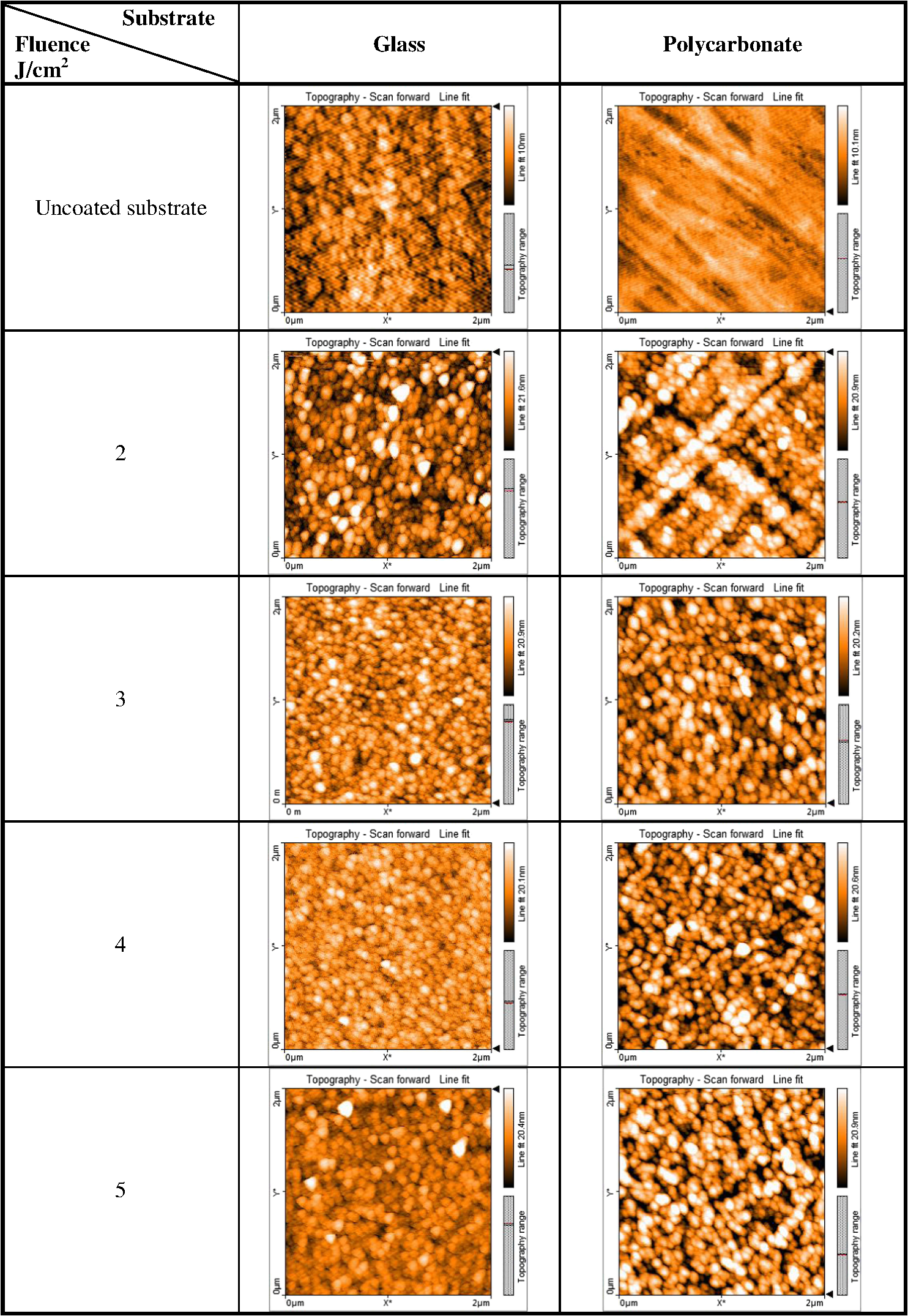 Table 1The morphology, optical, and electrical properties of Al-doped ZnO (AZO) films deposited on glass and polycarbonate (PC) at 2 to 5 J/cm2.
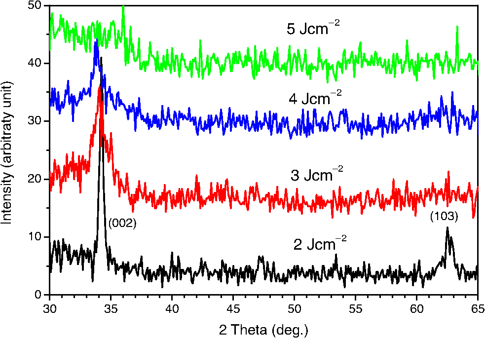
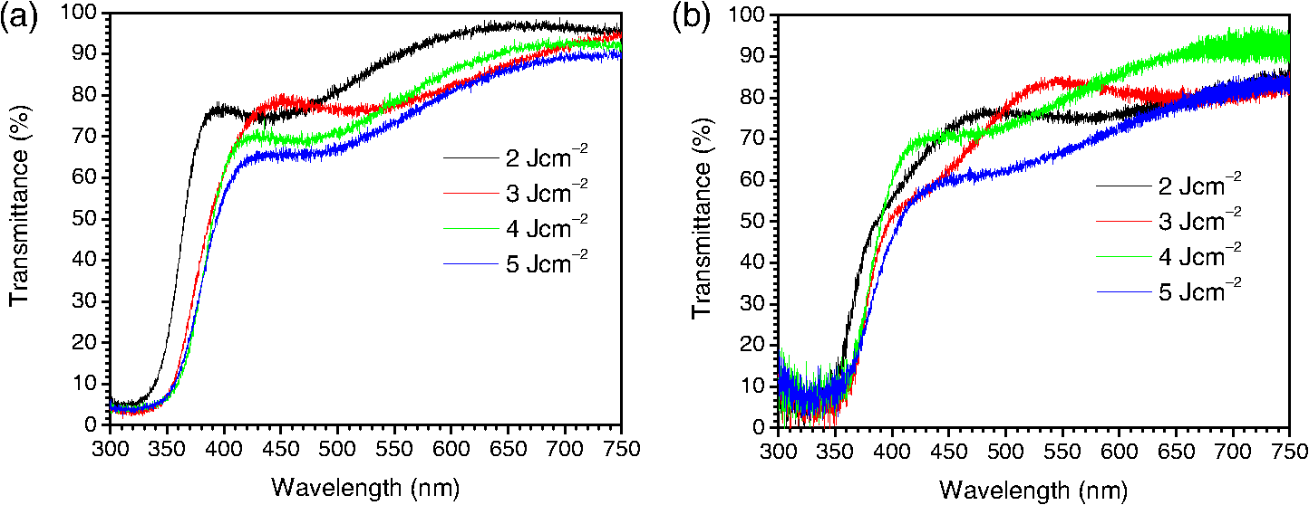
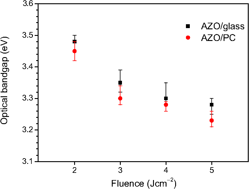
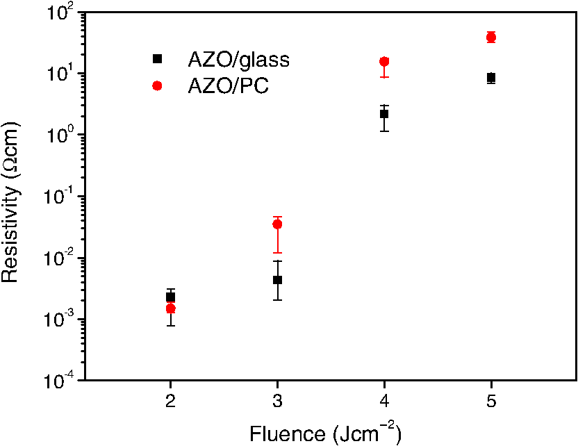
Figure 2 shows the XRD pattern of the AZO films deposited at 2 to . A sharp and most intense (002) and a small (103) reflection were observed for AZO deposited at . The sharp (002) reflection broadened with increasing laser fluence and diminished from AZO deposited at . The crystallinity of the films was highest for the sample deposited with , although the film is the thinnest. A slight shift was also observed when laser fluence increases. The broadening of the peak at higher fluence can be caused by smaller crystallite size and/or higher strain in the films. Figure 3 shows the optical transmittance spectra for AZO thin films on the glass and PC substrates at various laser fluences. The average transmittance of the films from 400 to 750 nm was about 80% on the glass substrate as compared with 75% on PC. The optical bandgap, , is deduced from a Tauc plot of versus based on Eq. (1) where is the constant and is the one-half for direct transition. for an AZO deposited at a different laser fluence on glass and the PC is shown in Fig. 4 and Table 1. There is a consistent decrease of when the laser fluence increased for AZO deposited on both substrates.The resistivity for the AZO films on glass and PC is shown in Fig. 5. The resistivities for AZO on glass and the PC increased up to four orders of magnitude with laser fluence. At high fluence, the resistivities of AZO on PC were higher than AZO on glass substrates. The best resistivity was obtained at for both glass and PC, where the values were for AZO on glass and for AZO on PC. Laser parameters such as pulse length and wavelength influence the ablation process, and subsequently the plume contents. Excimer lasers were normally used in deposition of ZnO, with shorter wavelength/higher photon energy3,4,9–12 that is able to produce highly energetic species than our current setup with a 355-nm laser. However, numerical results show that bombardment of ions with energy is capable to disturbed or displaced atoms in the growing films, which can potentially lead to crystallographic defects to the films.15 The lower photon energy and fluence in the current setup would minimize such an effect. In addition, rastering laser beams instead of the common rotating target approach would reduce continuous direct bombardment of ions onto the same spot. In a rastering laser beam, the laser beam and the created plasma plume scan across the target; therefore, the most intense part of the plasma plume arrived on a different part of the substrate. Whereas for a rotating target, only the target moves, the plasma plume will arrive onto the same position on the substrate. The method was reported to improve the morphology for the growth of AZO on polymer substrate, where the substrate is more susceptive to damage.11 On the other hand, we observed a rather low growth rate of the films as compared with deposition by excimer laser, which may be because of extensive optical excitation by a 355-nm laser. It is noted that 355-nm laser excitation can induce room temperature photoluminescence and even lasing action from a ZnO thin films or nanostructures.16–18 A 8-mm-thick bulk ZnO target optically pumped by a pulsed 355-nm laser lased above .18 The incident laser energy of the current setup may contribute to optical excitation, which affects the deposition efficiency. The low growth rate of is comparable with the reported value by a 355-nm deposition of ZnO.19 The deposited AZO films present satisfactory transmittance in the visible. The reduction of for AZO films deposited on glass and PC when fluence increased has also been observed in 248-nm deposition.12 The relation of the change in with carrier concentration is given by where is the effective mass for electrons and is the carrier concentration. Based on Eq. (2), the carrier concentration decreases when the change in with reference to an undoped ZnO film reduced. In our results, reduced with increasing laser fluence, and conductivity decreased with increasing fluence. The results suggest that the carrier concentration of the deposited AZO films, whether on glass or on PC, reduced when laser fluence increased, leading to low and low conductivity. In addition, based on the XRD results, crystallinity decreased as a laser fluence was increased. The results obtained here are compared with those deposited at similar conditions in Table 2. The best resistivities obtained here were one order of magnitude lower than those deposited by 248 nm with rastering a beam on PES and PET substrates,11 but close to those obtained on PET.12 It is also noted that the properties of AZO deposited by 355-nm laser are highly dependent on laser fluence, unlike in the case of 248-nm laser, where resistivities of can be obtained in a large fluence range of 1.5 to .Table 2Comparison of results from current work with reported values.
4.ConclusionIn this work, AZO thin films were deposited on glass and PC substrates at room temperature by using a 355-nm laser. The best films were obtained at , where the resistivities were for AZO on glass and for AZO on PC. The properties of AZO films on glass and PC were within the same range. At high fluence, AZO films with lower optical bandgap and higher resistivity were obtained ascribed to lower crystallinity and carrier density. The results also show a narrower fluence window for deposition of AZO films with resistivity of as compared with deposition by excimer lasers. AcknowledgmentsWe acknowledge the support from Telekom Malaysia (RDTC/130823) and the University of Malaya (BK019-2014). ReferencesZ. W. Liuet al.,
“Catalyst-free pulsed-laser-deposited ZnO nanorods and their room-temperature photoluminescence properties,”
Appl. Phys. Lett., 88
(5), 053110
(2006). http://dx.doi.org/10.1063/1.2168675 APPLAB 0003-6951 Google Scholar
D. Valeriniet al.,
“Zinc oxide nanostructures grown by pulsed laser deposition,”
Appl. Phys. A, 93
(3), 729
–733
(2008). http://dx.doi.org/10.1007/s00339-008-4703-z APAMFC 0947-8396 Google Scholar
S.-M. Parket al.,
“Structure and properties of transparent conductive doped ZnO films by pulsed laser deposition,”
Appl. Surf. Sci., 253
(3), 1522
–1527
(2006). http://dx.doi.org/10.1016/j.apsusc.2006.02.046 ASUSEE 0169-4332 Google Scholar
S. J. KangY. H. Joung,
“Optical and hall properties of Al-doped ZnO thin films fabricated by pulsed laser deposition with various substrate temperatures,”
J. Mater. Sci. Mater. Electron., 24
(6), 1863
–1868
(2013). http://dx.doi.org/10.1007/s10854-012-1024-y JSMEEV 0957-4522 Google Scholar
K.-S. KimH. W. KimC. M. Lee,
“Effect of growth temperature on ZnO thin film deposited on SiO2 substrate,”
Mater. Sci. Eng. B, 98
(2), 135
–139
(2003). http://dx.doi.org/10.1016/S0921-5107(02)00754-7 MSBTEK 0921-5107 Google Scholar
K. Matsubaraet al.,
“ZnO transparent conducting films deposited by pulsed laser deposition for solar cell applications,”
Thin Solid Films, 431–432 369
–372
(2003). http://dx.doi.org/10.1016/S0040-6090(03)00243-8 THSFAP 0040-6090 Google Scholar
H. Kimet al.,
“Transparent conducting aluminum-doped zinc oxide thin films for organic light-emitting devices,”
Appl. Phys. Lett., 76
(3), 259
(2000). http://dx.doi.org/10.1063/1.125740 APPLAB 0003-6951 Google Scholar
X. Q. Guet al.,
“Optical and electrical properties of ZnO:Al thin films synthesized by low-pressure pulsed laser deposition,”
Mater. Sci. Semicond. Process., 14
(1), 48
–51
(2011). http://dx.doi.org/10.1016/j.mssp.2011.01.003 MSSPFQ 1369-8001 Google Scholar
K. Matsubaraet al.,
“Room-temperature deposition of Al-doped ZnO films by oxygen radical-assisted pulsed laser deposition,”
Thin Solid Films, 422
(1–2), 176
–179
(2002). http://dx.doi.org/10.1016/S0040-6090(02)00965-3 THSFAP 0040-6090 Google Scholar
H. Aguraet al.,
“Low resistivity transparent conducting Al-doped ZnO films prepared by pulsed laser deposition,”
Thin Solid Films, 445
(2), 263
–267
(2003). http://dx.doi.org/10.1016/S0040-6090(03)01158-1 THSFAP 0040-6090 Google Scholar
J. Kimet al.,
“Electric properties and surface characterization of transparent Al-doped ZnO thin films prepared by pulsed laser deposition,”
Thin Solid Films, 516
(16), 5223
–5226
(2008). http://dx.doi.org/10.1016/j.tsf.2007.07.095 THSFAP 0040-6090 Google Scholar
M. Girtanet al.,
“On the properties of aluminium doped zinc oxide thin films deposited on plastic substrates from ceramic targets,”
Appl. Surf. Sci., 274 306
–313
(2013). http://dx.doi.org/10.1016/j.apsusc.2013.03.046 ASUSEE 0169-4332 Google Scholar
Y. LiuQ. LiH. Shao,
“Properties of ZnO:Al films deposited on polycarbonate substrate,”
Vacuum, 83
(12), 1435
–1437
(2009). http://dx.doi.org/10.1016/j.vacuum.2009.05.006 VACUAV 0042-207X Google Scholar
E. Holmelundet al.,
“Pulsed laser deposition of aluminum-doped ZnO films at 355 nm,”
Appl. Phys. A, 79
(4–6), 1137
–1139
(2004). http://dx.doi.org/10.1007/s00339-004-2663-5 APAMFC 0947-8396 Google Scholar
J. Perrièreet al.,
“Comparison between ZnO films grown by femtosecond and nanosecond laser ablation,”
J. Appl. Phys., 91
(2), 690
(2002). http://dx.doi.org/10.1063/1.1426250 JAPIAU 0021-8979 Google Scholar
P. Zuet al.,
“Ultraviolet spontaneous and stimulated emissions from ZnO microcrystallite thin films at room temperature,”
Solid State Commun., 103
(8), 459
–463
(1997). http://dx.doi.org/10.1016/S0038-1098(97)00216-0 SSCOA4 0038-1098 Google Scholar
H. Caoet al.,
“Ultraviolet lasing in resonators formed by scattering in semiconductor polycrystalline films,”
Appl. Phys. Lett., 73
(25), 3656
(1998). http://dx.doi.org/10.1063/1.122853 APPLAB 0003-6951 Google Scholar
R. K. TharejaA. Mitra,
“Random laser action in ZnO,”
Appl. Phys. B, 71
(2), 181
–184
(2000). http://dx.doi.org/10.1007/s003400000274 APBOEM 0946-2171 Google Scholar
T. HiraideS. KurumiK. Suzuki,
“p-type zinc oxide films grown by infrared-light-assisted pulsed laser deposition,”
Appl. Phys. A, 110
(4), 963
–966
(2013). http://dx.doi.org/10.1007/s00339-012-7228-4 APAMFC 0947-8396 Google Scholar
E. L. Papadopoulouet al.,
“Undoped and Al-doped ZnO films with tuned properties grown by pulsed laser deposition,”
Thin Solid Films, 516
(22), 8141
–8145
(2008). http://dx.doi.org/10.1016/j.tsf.2008.04.022 THSFAP 0040-6090 Google Scholar
BiographyKwan Chu Tan is currently pursuing a MEng Sci degree in the area of pulsed laser deposition and laser patterning of organic electronics. Seong Ling Yap received her PhD in plasma physics from the University of Malaya. Her research interests include pulsed plasma application and diagnostic, plasma medicine and novel plasma source as a sustainable technology. Soon Yie Kok is currently pursuing a MEng Sci degree in the area of pulsed laser deposition and laser patterning of organic electronics. Wee Ong Siew received a BSc and an MSc in the area of laser technology, and a PhD in laser materials interaction. His research interests include laser-induced phenomena, laser electronics, and optics. Teck Yong Tou is currently a professor with the Faculty of Engineering, Multimedia University, Malaysia. He received his BSc and PhD degrees in physics from the University of Malaya, Malaysia, in 1982 and 1987, respectively. His current research interests include OLED, laser-matter interactions and materials processing, thin film deposition and nanoparticle generation, solder joint integrity. Seong Shan Yap is an associate professor with University of Malaya. She received her BSc in physics, MTech in materials science, and PhD in engineering. She is a member of SPIE. Her research interests include laser processing of nanomaterials for application in OLED and solar cell, DLC, Ge/Si nanostructures and semiconducting polymer. |
||||||||||||||||||||||||||||||||||||||||||||||||||||||||||||||||||||||||||||||||||||||||||||||||||||||||||||||||||||||||||||||||||||||||||||||||||||||||||||||||||||||||||||||||||||||||||||||