
|
|
1.IntroductionThe molecular beam epitaxy (MBE) grown InGaN/GaN-based nanowires heterostructure is attractive as it can be grown spontaneously on a highly mismatched surface, such as silicon,1–5 oxides,6–9 and metal,10–13 without threading dislocations.14,15 In the planar III-nitride material system, random alloy fluctuations and phase segregation of In during the growth of the InGaN layer result in the formation of In-rich clusters.16–18 These clusters result in a separate recombination center with distinct behavior compared with the typical surrounding InGaN matrix. The optical properties of these clusters have been studied in planar structures utilizing both conventional optical microphotoluminescence () measurement19–21 and high-resolution cathodoluminescence scanning transmission electron microscopy (CL-STEM).22,23 For closely packed quantum-disks ()-in-nanowires structures, the diffraction-limited conventional optical characterization method24 can only provide macroscopic characteristics of the nanowires ensemble. As the localization centers are typically only several nanometers in size, results obtained through a conventional optical method do not provide enough information on the nature of individual recombination centers. Accurate study of localization centers within nanowires structures is further complicated due to unique nanowires characteristics, such as surface-state-related Fermi-level pinning25,26 and nonuniform strain distribution.27–30 Although cathodoluminescence scanning electron microscopy has previously been utilized to spatially characterize the emission characteristics of nanowires structures, the structural characterization is limited to only the surface of the nanowires, and the resolution is not adequate to probe individual nanoscale-sized recombination centers embedded inside the active region of the nanowires.31,32 CL-STEM on the other hand is suitable for probing the nanoscale optical properties of nanowires because of the small interaction volume and high resolution resulting from the high acceleration voltage used.33–35 Through utilizing CL-STEM, it is possible to simultaneously retrieve both the optical and structural features of the nanowires while at the same time utilizing a high-angle annular dark field (HAADF), providing a thorough understanding of how structural features and luminescence properties of nanowires affect each other. This capability has been demonstrated to investigate the nanoscale optical properties of nanowire heterostructures,22,36 with features as small as nanometer-sized clusters.37 In this study, we characterized the nature of competing recombination centers inside InGaN/GaN -in-nanowires heterostructure using both macroscopic and nanoscale optical characterization. Initial measurement indicates the existence of separate recombination centers with distinct characteristics from the average -related emission. To further elucidate the results, we utilized CL-STEM to spatially resolve the origin of two distinct recombination centers from the active region of the -in-nanowires heterostructure. CL spectra acquisition over an ensemble of nanowires correlates well with the measurement. CL-STEM accurately pinpointed with nanoscale accuracy the location of a separate recombination center embedded alongside the , referred to as the nanoclusters-related recombination center henceforth. High-resolution point acquisition on a single nanoclusters-related recombination center shows that at 100 K, an individual nanoclusters-related recombination center has a narrow linewidth, in the range of . We thus established a direct visualization of embedded nanoclusters-related emission and its relation to the structure of the nanowires. Our work gives insight on the optical and structural properties of simultaneously coexisting nanoscale luminescence sites within nanowires heterostructures. 2.Experimental Details2.1.Nanowires GrowthThe -in-nanowires samples were grown catalyst-free using plasma-assisted molecular beam epitaxy on a Si(111) substrate. Before growth, the substrate was cleaned using dilute hydrofluoric acid to remove any native oxide and was then loaded immediately into the MBE chamber. After loading, the substrate was heated at 600°C and 900°C to desorb the organic material and any remaining native oxide, respectively. The structure consists of an -type Si-doped GaN base, an active region with eight stacks of the InGaN and GaN barrier, and a -type Mg-doped GaN top layer. The -GaN base of the nanowires was grown at 720°C, and the top p-GaN layer was grown at 640°C. Eight pairs of the InGaN and GaN barriers were grown at for the low temperature (LT) sample and for the high temperature (HT) sample with a constant In/Ga flux ratio throughout the growth. The typical thickness was for the silicon-doped -GaN base and for the Mg-doped -GaN top. The thicknesses of the InGaN and GaN barrier were and , respectively. 2.2.Material CharacterizationThe first low-temperature measurements were conducted using a confocal micro-Raman spectrometer (Horiba/Jobin Yvon Aramis) with a 325-nm He–Cd laser as the excitation source. The samples were placed inside a cryostat cell (Linkam, THMS 600), and the temperature was changed from 77 to 300 K with a stability of . To investigate the -shape behavior of peak emission energy, second low-temperature measurements were conducted using a continuous helium flow cryostat (Janis). The system was then cooled down to 10 K, and the temperature was raised by 10 K steps to 150 K. The sample was excited using a 405-nm laser with a 0.5-mW excitation power and a spot size. The TEM samples were prepared by physical removal of the nanowires before drop casting the nanowires onto lacey carbon TEM grids. High-resolution HAADF STEM images and the cathodoluminescence signal were recorded simultaneously using a Gatan HAADF detector. Cathodoluminescence measurements were performed in a JEOL 2100F TEM operating at an acceleration voltage of 80 kV and probe current in the order of 200 pA in STEM mode using a Gatan Vulcan™ system. The acceleration voltage was chosen as the lowest possible to minimize beam damage.38 A specially designed cryogenic holder includes ellipsoidal mirrors above and below the specimen to reflect the cathodoluminescence into optical fibers, which guide the light out of the TEM to a light detection system. The light detection system includes fast integrated intensity mapping using a photomultiplier tube (PMT) and, for spectral analysis, a Czerny–Turner optical spectrometer fitted with charge-coupled device (CCD) and PMT. The read out of the CCD can be performed synchronously with the scanning of the e-beam-enabling hyperspectral data acquisition. The electron probe size was on the order of 0.5 nm. Considering the Bohr exciton radius of GaN, the upper limit of the CL-STEM is defined as 5 nm. The spectral resolution was for CL spectrum images and can be as low as 0.5 nm depending on the slit width used; the samples were cooled to by liquid nitrogen unless otherwise stated. 3.Results and DiscussionSEM micrographs for the nanowires array from the LT sample are shown in Figs. 1(a) and 1(b). The nanowires density calculated statistically is . The HAADF STEM image of a single nanowire with embedded is shown in Fig. 1(c). The typical length of the nanowires is , and the top lateral width is . The typical thickness of the is . The nanowires grow perpendicular to the substrate with an inversely tapered morphology. The tapering is caused by the reduction of growth temperature during InGaN growth to promote In incorporation, resulting in lower adatom diffusion length and preferential lateral growth. A degree of coalescence can be observed on the top part of the nanowires, which is caused by expansion of the diameter of the nanowires as they grow. Fig. 1Electron microscopy micrograph of the nanowires from LT sample. (a) Plan-view SEM micrograph of the nanowires grown on silicon, (b) the corresponding cross-section view of the nanowires, and (c) HAADF image of a single nanowire with eight InGaN (as indicated). 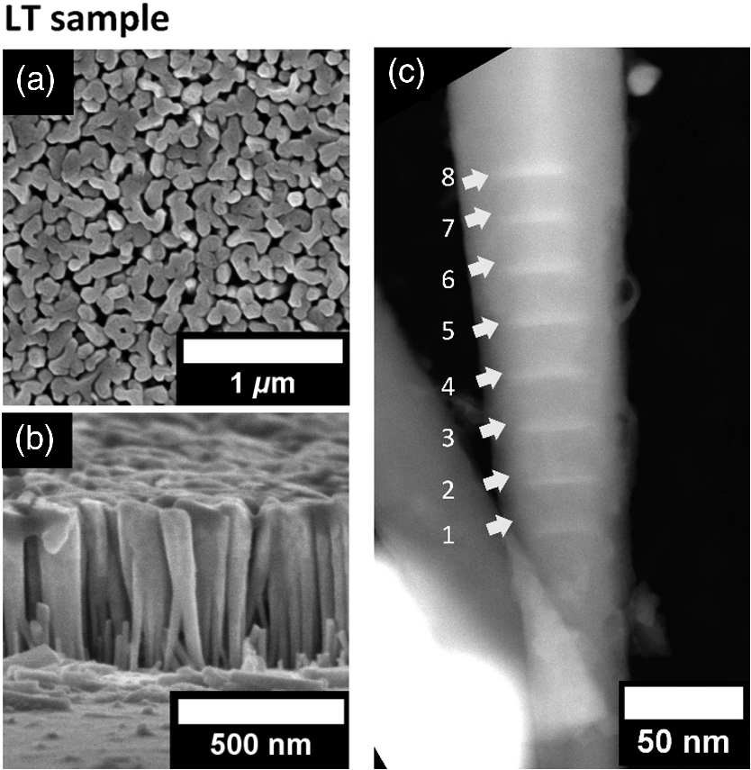 3.1.Microphotoluminescence CharacterizationTo investigate the luminescence characteristics of the nanowires, ensemble spectra were taken using a 325-nm He–Cd laser in a backscattering configuration. Temperature-dependent measurements were performed between 77 and 300 K. For the LT sample, at room temperature, only the green emission at 546 nm is observed. However, when the sample is measured at 77 K [Fig. 2(a)], an additional blue peak emitting at 465 nm is visible. The blue emission peak is observed to quench faster than the green emission peak as the temperature increases. From this observation, it is possible that the blue peak is attributed to shallower recombination centers. For comparison, a second nanowires sample with a higher active region growth temperature and a nominally smaller In composition (the HT sample) was grown. The temperature-dependent result from the HT sample is shown in Fig. 2(b), where only a single dominant peak can be observed at both 77 and 300 K. Fig. 2emission spectra taken at 77 and 300 K using 325 nm excitation for (a) an LT sample () and (b) an HT sample (). The full width at half maximum values are shown within the bracket. In the LT sample, the blue peak is quenched at room temperature, while the green peak remains stable. Additional temperature-dependent measurement using helium-cooled cryostat from 10 to 150 K with 405 nm excitation was done to obtain (c) the peak shift of the LT sample versus temperature, showing the -curve associated with In clustering and (d) the integrated intensity versus temperature of blue and green peaks. 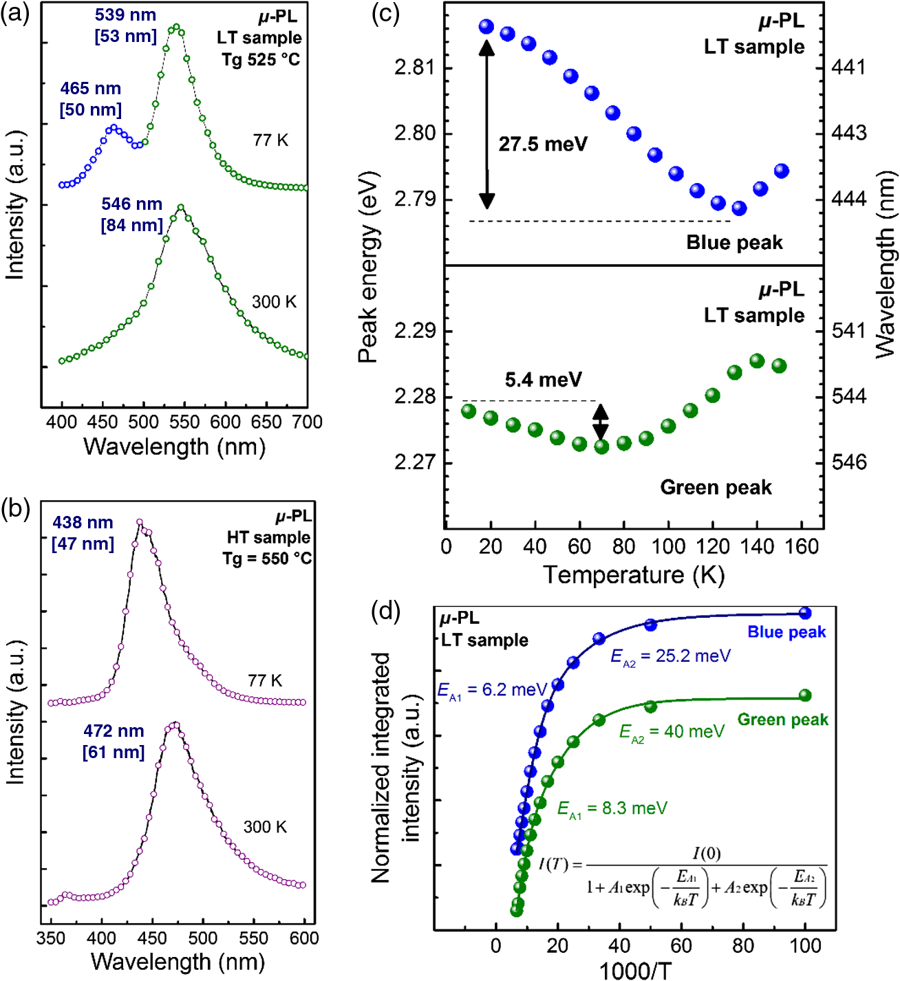 We further investigate the behavior of these two recombination centers through a separate temperature-dependent measurement, using a 405-nm diode laser as the excitation source with temperature ranging from 10 to 150 K on the LT sample. In Fig. 2(c), the peak position versus temperature is shown, with the blue peak redshifting by 27.5 meV up to 130 K, followed by a blueshift, and the green peak redshifting by 5.4 meV until 70 K, followed by blueshift until 140 K, and another redshift. For both the blue and green emissions, the positions of their peak intensities follow the S-shape associated with In clustering in the active region.39 The initial redshift can be explained as carriers moving to deeper recombination centers with smaller bandgap via carrier hopping. After reaching equilibrium, the carriers can start filling the higher energy states, represented by the blueshifting of the peak wavelength. Finally, the redshifting can be explained by the regular thermionic emission of the carriers. The S-shape confirms that both peaks originate from carrier population and depopulation within the insertions in the active region and not from defects.40 Figure 2(d) shows the change of integrated intensity with temperature. By applying a two-component Arrhenius equation (inset), the activation energies and of the blue peak are determined to be 6.2 and 25.2 meV, whereas the activation energies of the green peak are 8.3 and 40 meV. The activation energy indicates the energy barrier that must be overcome before carriers escape radiative recombination centers and recombine nonradiatively. The lower activation energy of the blue peak indicates that carriers within the blue recombination center are more susceptible to thermal quenching due to the activation of nonradiative recombination centers and nonradiative recombination on the surface of the nanowires. On the other hand, the higher activation energy in the green peak shows a deeper localized state, as evidenced by the stable green emission even when measured at room temperature. Despite being a useful tool to quantify various optical parameters of the recombination centers within the nanowires, the results obtained represent the statistical average of an ensemble of nanowires. Furthermore, it does not give any direct correlation on how the structural properties of the nanowires affect the recombination centers embedded inside. To investigate the characteristics of individual nanometer-sized recombination centers, a cathodoluminescence measurement with nanoscale excitation capability is required. 3.2.Cathodoluminescence Scanning Transmission Electron Microscopy CharacterizationNanoscale luminescence characterization was conducted by CL-STEM. We first attempted to use CL-STEM to verify the validity of the two distinct recombination centers observed using low-temperature . By scanning the beam over an entire nanowires ensemble, a spectrum response analogous to the measurement can be obtained. The CL-STEM measurement was implemented both at room temperature and at 100 K for the LT sample. The ensemble spectra of the LT sample [Figs. 3(a) and 3(b)] confirm that at room temperature, only a single peak emitting at 518 nm can be detected, whereas two distinct peaks at 444 and 540 nm can be observed at 100 K; this result agrees well with the measurement. The CL spectrum of the nanowires ensemble at 100 K exhibits broader linewidth than the measurement result at 77 K due to phonon broadening at increased temperature. At room temperature, the CL spectrum peak linewidth is relatively narrower compared with the spectrum and is blueshifted. The narrower linewidth is caused by the smaller number of nanowires excited using CL compared with the measurement; thus, less compositional inhomogeneity is observed. Based on the nanowire density and beam spot size, nanowires are excited using , whereas 100 to 150 nanowires are excited during ensemble CL measurement. The excited electron-hole pairs can cause blueshifting through a combination of Coulomb screening (thus reducing the quantum-confined Stark effect) and band-filling effect.41 In general, CL excitation generates more electron-hole pairs compared with PL excitation,42 which results in a more pronounced blueshift compared with the PL result. Fig. 3Comparison of CL-STEM measurement between a nanowires ensemble from LT sample. CL spectra of electron beam scanned over an ensemble of nanowires for (a) low-temperature measurement and (b) room temperature measurement. The inset shows the HAADF image of the ensemble of nanowires. (c) HAADF image and (d) the corresponding true color CL mapping from a single nanowire, showing a spatially localized blue emission at 100 K. (e) Bandpass-filtered monochromatic image from the CL emission map centered at 460 nm. (f) Point acquisition CL emission spectrum measured at the region of the blue emission. (g) HAADF image with overlaid red dashed lines showing the outline of the nanowire and the position of . The corresponding bandpass-filtered CL-STEM images at 100 K showing emission at (h) 406 nm, (i) 420 nm, (j) 445 nm, (k) 457 nm, (l) 510 nm, and (m) 530 nm. A strong emission at , which spatially coincides with the branching, can be observed in (k). Although the actual size of the localization center is only several nanometers, carrier diffusion in the order of 30 to 40 nm makes the center appears larger. 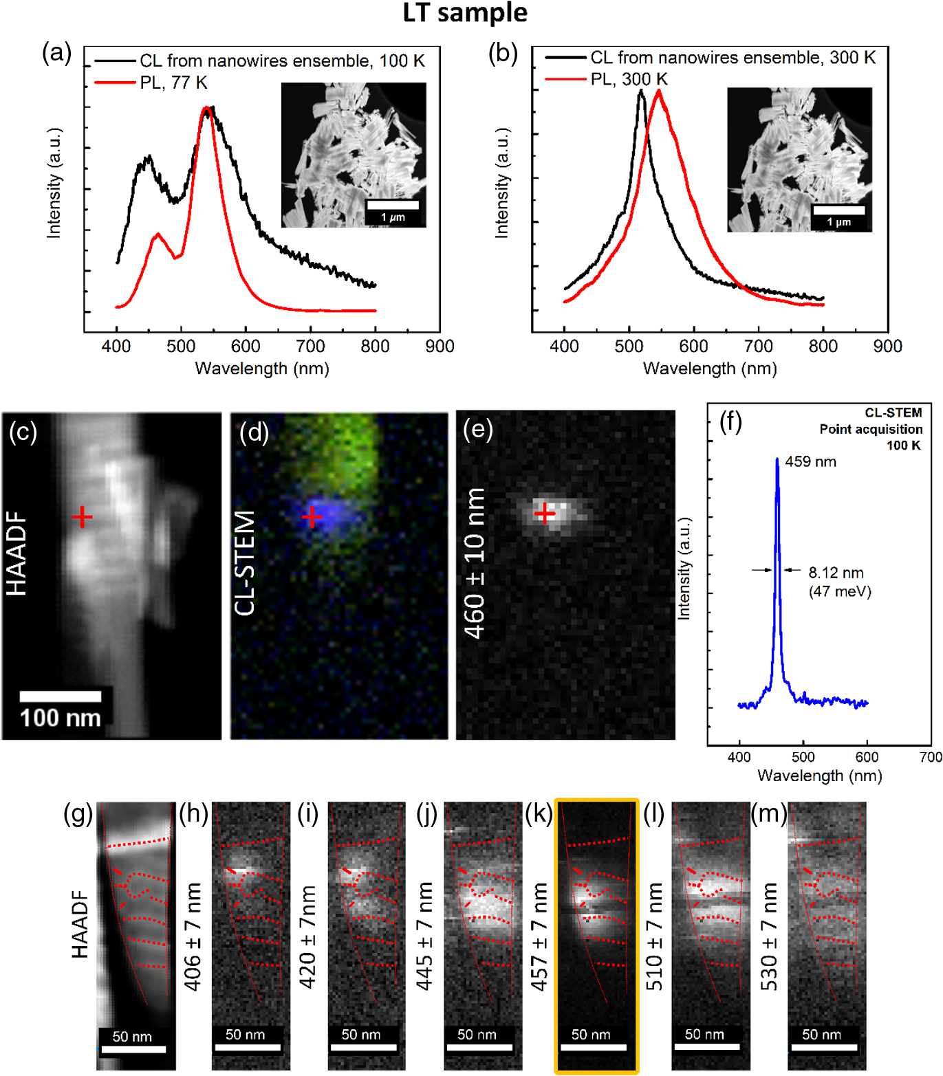 Figures 3(c)–3(e) show an HAADF image of a single nanowire with the corresponding CL true color map, where the color of each pixel in the hyperspectral data cube is chosen to represent the data by comparing the measured spectrum to a standardized color chart. It is implied that the blue emission is spatially localized within a single region of the nanowire, whereas the green emission is relatively delocalized. Interestingly, the bright blue nanoclusters-related emission can coexist with the -related green emission within a single nanowire and occupy only a localized area. Although the actual size of the localization center is only several nanometers, carrier diffusion of the electron-beam-generated electron–hole pair makes the center appear larger. From its spatial extent, the carrier diffusion within the recombination center is estimated to be 30 to 40 nm before they recombine. A detailed point acquisition on a single segregation-related recombination center within the LT sample was performed. The red cross in Figs. 3(c)–3(e) indicates where the CL spectrum was acquired. The result in Fig. 3(f) shows a CL spectrum with a single peak and relatively narrow linewidth of (47 meV), compared with the broad twin peak CL spectrum from nanowires ensemble measurement in Fig. 3(a). This result demonstrates the importance of CL-STEM for probing the optical property of a single nanoscale-sized localization center within a nanowires structure and correlating it with the ensemble optical properties. Further characterization was performed by overlaying a band-pass-filtered CL spectra on top of the HAADF image, shown in Figs. 3(g)–3(m). The InGaN alloy within the nanowire is outlined with a red dashed line for clarity. It is shown that branching and clustering occur within the nanowire. In Fig. 3(k), a bright and spatially localized emission at can be observed. The blue emission coincides with the location of the branching, which suggests that these blue-colored recombination centers appear when irregularities, such as branching and nanoclusters, are present in the InGaN . By contrast, the emission from other parts of the nanowires, corresponding to -related emission, is relatively weak and delocalized. For comparison, we have also performed HAADF imaging and CL-STEM measurement at 100 K on the HT sample, shown in Fig. 4(a). The CL spectrum obtained from an ensemble of nanowires shows only a single peak emitting at 470 nm, which correlates well with the measurement. As indicated in the true color map of a typical nanowire shown in Fig. 4(c), the dominant blue emission comes from a weakly localized -related recombination center. The blue emission is uniform across the active region with no spatially localized bright emission from the nanoclusters-related recombination center. Fig. 4(a) CL spectrum of electron beam scanned over an ensemble of nanowires, for an HT sample. The inset shows HAADF image of the nanowires ensemble. (b) HAADF image of a single nanowire from HT sample with (c) the corresponding true color CL mapping. 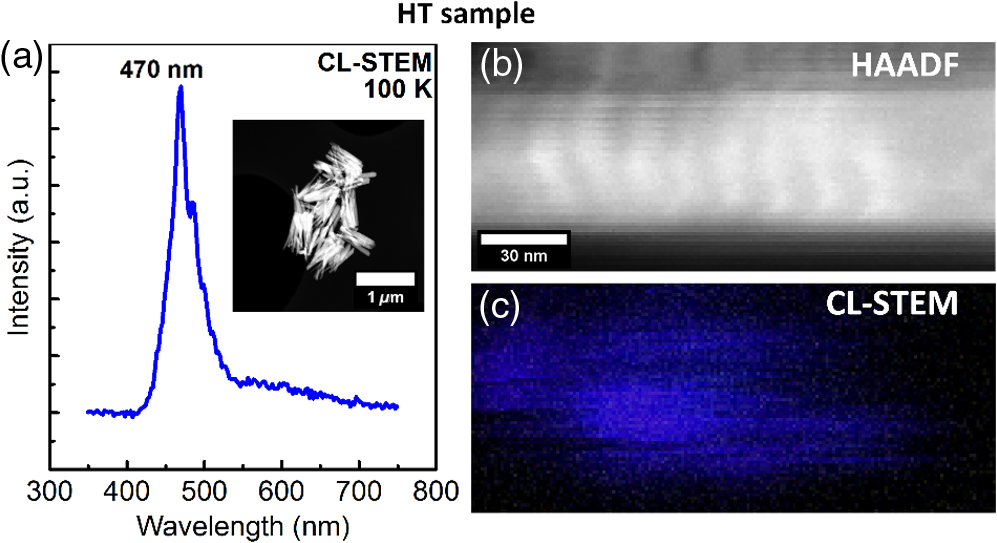 From what we have observed, we deduced that there are mainly two distinct recombination centers within the LT nanowires sample, namely the nanoclusters-related recombination center, which arises due to the formation of nanoclusters, and the -related recombination center, which is relatively weaker at low measurement temperatures and is delocalized. The blue emission in the LT sample revealed by measurement originates from nanoclusters-related recombination centers, as evidenced by the strong spatial localization seen in CL-STEM measurements. As the size of the are comparable to the electron radius inside InGaN, and both peaks exhibit the -shaped peak emission shift related to exciton population and depopulation processes,39 we believe that both emission peaks come from bound excitonic recombination. At lower measurement temperature, some of these nanoclusters-related recombination centers are filled with carriers. As the temperature increases, the emission from these recombination centers is redshifted and quenched, due to excitons dissociating into free carriers and obtaining sufficient energy and escape into the surrounding InGaN by thermionic emission, thereby depopulating the nanoclusters-related recombination centers. This process is reflected by the low activation energy value of the blue peak. Emission from free-carrier recombination typically has a longer PL decay time compared with excitonic recombination.43 Further time-resolved PL study is required to investigate the contribution of free-carrier recombination toward the overall emission. With the nanoclusters depopulated and most of the recombination mechanisms happening within the , the spectrum is dominated by the green -related peak at room temperature. To rule out thickness variations and different In compositions as the cause of the two separate peaks, we have performed additional numerical simulation and electron energy loss spectroscopy (EELS) spectrum acquisition. Numerical simulation of the effect of thickness on emission wavelength was done using a commercial Nextnano3 software package.44 For our model, we use a simple one-dimensional InGaN quantum well with variable thicknesses between GaN barriers. The quantum-confined Stark effect is assumed to be negligible considering strain relaxation from the . The InGaN well simulated has a 35% In content, resulting in peak emission of 2.3 eV at 6 nm, which agrees well with the measured PL emission. We then calculate the transition energy of the electron-hole ground state. From the simulation result shown in Fig. 5, we can see that for InGaN wells above 5-nm thick, the transition energy is relatively insensitive to thickness variation within the InGaN well. As the blue and green emission peak energies are separated by more than 500 meV, we can infer that thickness variation between is not the main cause for the blue emission. Fig. 5Calculated transition energy of the electron-hole ground state of an InGaN well inserted between GaN barriers for different well thickness. 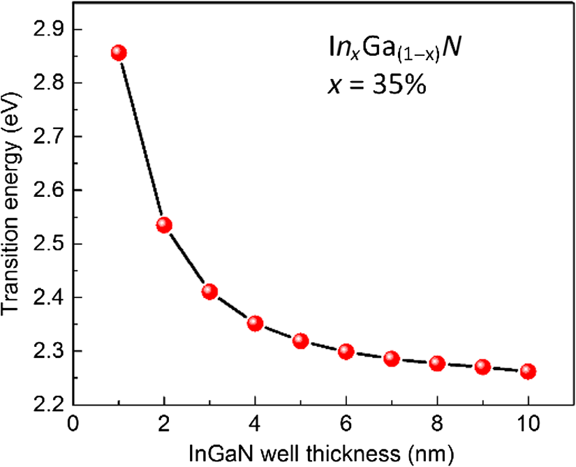 An HAADF image of two nanowires from an LT sample aligned horizontally side by side, referred to as nanowire 1 and nanowire 2, along with the corresponding CL true color map and multiple linear least squares–fitted EELS spectrum image for In content are shown in Figs. 6(a)–6(c). We detected the existence of simultaneous blue and green emissions within nanowire 1. In addition, we have also detected a strong blueshifted emission emitting from the sidewall region of nanowire 2, indicated by a red box in Fig. 6(b). However, even with the existence of simultaneous blue and green emission within a single nanowire and strongly localized blueshifted emission, the In composition across the nanowire is relatively constant within a few atomic percentage. Therefore, we can also confirm that the blueshifted emission is likely not caused by compositional variation between . Fig. 6(a) HAADF image of region of two nanowires from the LT sample aligned horizontally with the corresponding (b) true color CL map and (c) EELS spectrum image for In composition. A bright localized emission from the sidewall region of the nanowire is indicated by a red square in (b). EELS result indicates that the In composition is relatively constant within a few atomic percentage across single nanowire. 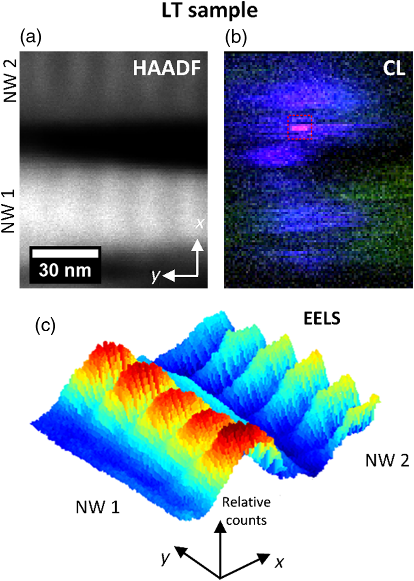 In contrast to the LT sample, the HT sample only has emission coming from -related recombination centers. Therefore, even at low measurement temperatures, only a single dominant peak can be observed. The redshift observed with the peak wavelength with increasing temperature is due to temperature-dependent bandgap shrinking common in semiconductor materials.45 The irregularities within the , which give rise to nanocluster-related emission, are thought to arise due to In segregation because of lower In miscibility at a lower growth temperature, leading to the formation of the nanoclusters. The nanoclusters-related emission center is more prominent in the LT sample, where the are grown at relatively lower temperature. Although an individual nanocluster typically exhibits narrow emission linewidth, the blue emission is broader for both μ-PL and nanowires ensemble CL acquisition due to size and composition distribution between separate nanoclusters. By contrast, the inside the HT sample are grown at a higher temperature, resulting in the formation of with better crystal quality and reduced In clustering, indicated by the absence of spatially localized emission. By using CL-STEM, we have observed two distinct emissions within InGaN/GaN nanowires heterostructures with nanoscale resolution and spatially identified the origin of each recombination centers. 4.SummaryIn conclusion, a detailed investigation on the origin of two distinct recombination centers within -in-nanowires heterostructure was performed utilizing both and nanoscale CL-STEM. From the measurements, we identify the existence of two recombination centers within the active region of the nanowires. CL-STEM from a single nanowire confirms that the emission corresponds to concurrent spatially localized InGaN nanoclusters-related emission and delocalized emissions from the region. A high-resolution scan on a single nanowire reveals that the nanoclusters-related recombination center corresponds to irregularities within , i.e., branching and clustering. Such irregularities are thought to arise from the low miscibility of In at a lower growth temperature. In contrast, such nanoclusters-related recombination centers are mostly absent from the HT sample. We have also ruled out the possibility of thickness variation and compositional variation across as the cause of the additional emission peak by performing numerical simulation and EELS acquisition, respectively. By utilizing CL-STEM, it is possible to obtain a thorough understanding of the relation between the structure of InGaN/GaN nanowires and its optical properties with nanoscale accuracy. Our results confirm that distinct nanoclusters-related recombination centers exist simultaneously with the -related recombination center within the InGaN/GaN heterostructure under particular growth conditions. AcknowledgmentsWe acknowledge the financial support from King Abdulaziz City for Science and Technology (KACST), Grant No. KACST TIC R2-FP-008. This publication is also based on work supported by the King Abdullah University of Science and Technology (KAUST) baseline funding BAS/1/1614-01-01. The authors also acknowledge Experimental Technique Centre of Brunel University London for granting us access to the CL measurement facility. ReferencesL. H. Robins et al.,
“Optical and structural study of GaN nanowires grown by catalyst-free molecular beam epitaxy. II. Sub-band-gap luminescence and electron irradiation effects,”
J. Appl. Phys., 101
(11), 113506
(2007). http://dx.doi.org/10.1063/1.2736266 JAPIAU 0021-8979 Google Scholar
M. Tchernycheva et al.,
“Growth of GaN free-standing nanowires by plasma-assisted molecular beam epitaxy: structural and optical characterization,”
Nanotechnology, 18
(38), 385306
(2007). http://dx.doi.org/10.1088/0957-4484/18/38/385306 NNOTER 0957-4484 Google Scholar
F. Furtmayr et al.,
“Nucleation and growth of GaN nanorods on Si (111) surfaces by plasma-assisted molecular beam epitaxy—the influence of Si- and Mg-doping,”
J. Appl. Phys., 104
(3), 034309
(2008). http://dx.doi.org/10.1063/1.2953087 JAPIAU 0021-8979 Google Scholar
R. Calarco et al.,
“Nucleation and growth of GaN nanowires on Si(111) performed by molecular beam epitaxy,”
Nano Lett., 7
(111), 2248
–2251
(2007). http://dx.doi.org/10.1021/nl0707398 NALEFD 1530-6984 Google Scholar
O. Landré et al.,
“Nucleation mechanism of GaN nanowires grown on (111) Si by molecular beam epitaxy,”
Nanotechnology, 20
(41), 415602
(2009). http://dx.doi.org/10.1088/0957-4484/20/41/415602 NNOTER 0957-4484 Google Scholar
H. Hayashi, Y. Konno and K. Kishino,
“Self-organization of dislocation-free, high-density, vertically aligned GaN nanocolumns involving InGaN quantum wells on covered with a thin AlN buffer layer,”
Nanotechnology, 27
(5), 55302
(2016). http://dx.doi.org/10.1088/0957-4484/27/5/055302 NNOTER 0957-4484 Google Scholar
W. Wang et al.,
“Epitaxial growth of GaN films on unconventional oxide substrates,”
J. Mater. Chem. C, 2
(44), 9342
–9358
(2014). http://dx.doi.org/10.1039/C4TC01655F Google Scholar
V. Kumaresan et al.,
“Self-induced growth of vertical GaN nanowires on silica,”
Nanotechnology, 27
(13), 135602
(2016). http://dx.doi.org/10.1088/0957-4484/27/13/135602 NNOTER 0957-4484 Google Scholar
S. Zhao et al.,
“Growth of large-scale vertically aligned GaN nanowires and their heterostructures with high uniformity on SiO(x) by catalyst-free molecular beam epitaxy,”
Nanoscale, 5
(12), 5283
–5287
(2013). http://dx.doi.org/10.1039/c3nr00387f NANOHL 2040-3364 Google Scholar
M. Wölz et al.,
“Epitaxial growth of GaN nanowires with high structural perfection on a metallic TiN film,”
Nano Lett., 15
(6), 3743
–3747
(2015). http://dx.doi.org/10.1021/acs.nanolett.5b00251 NALEFD 1530-6984 Google Scholar
G. Calabrese et al.,
“Molecular beam epitaxy of single crystalline GaN nanowires on a flexible Ti foil,”
Appl. Phys. Lett., 108
(20), 202101
(2016). http://dx.doi.org/10.1063/1.4950707 APPLAB 0003-6951 Google Scholar
B. J. May, A. T. M. G. Sarwar and R. C. Myers,
“Nanowire LEDs grown directly on flexible metal foil,”
Appl. Phys. Lett., 108
(14), 141103
(2016). http://dx.doi.org/10.1063/1.4945419 APPLAB 0003-6951 Google Scholar
C. Zhao et al.,
“Facile formation of high-quality InGaN/GaN quantum-disks-in-nanowires on bulk-metal substrates for high-power light-emitters,”
Nano Lett., 16
(2), 1056
–1063
(2016). http://dx.doi.org/10.1021/acs.nanolett.5b04190 NALEFD 1530-6984 Google Scholar
S. D. Hersee et al.,
“Threading defect elimination in GaN nanowires,”
J. Mater. Res., 26
(17), 2293
–2298
(2011). http://dx.doi.org/10.1557/jmr.2011.112 JMREEE 0884-2914 Google Scholar
R. Colby et al.,
“Dislocation filtering in GaN nanostructures,”
Nano Lett., 10
(5), 1568
–1573
(2010). http://dx.doi.org/10.1021/nl9037455 NALEFD 1530-6984 Google Scholar
D. Gerthsen et al.,
“Composition fluctuations in InGaN analyzed by transmission electron microscopy,”
Phys. Status Solidi, 177
(1), 145
–155
(2000). http://dx.doi.org/10.1002/(ISSN)1521-396X PHSSAK 0031-8957 Google Scholar
P. Ruterana et al.,
“Composition fluctuation in InGaN quantum wells made from molecular beam or metalorganic vapor phase epitaxial layers,”
J. Appl. Phys., 91
(11), 8979
–8985
(2002). http://dx.doi.org/10.1063/1.1473666 JAPIAU 0021-8979 Google Scholar
Y. Narukawa et al.,
“Role of self-formed InGaN quantum dots for exciton localization in the purple laser diode emitting at 420 nm,”
Appl. Phys. Lett., 70
(8), 981
–983
(1997). http://dx.doi.org/10.1063/1.118455 APPLAB 0003-6951 Google Scholar
F. Wang et al.,
“Green and blue emissions in phase-separated InGaN quantum wells,”
J. Appl. Phys., 114
(16), 163525
(2013). http://dx.doi.org/10.1063/1.4827205 JAPIAU 0021-8979 Google Scholar
H. Sun et al.,
“Transfer and recombination mechanism of carriers in phase-separated InGaN quantum wells,”
J. Appl. Phys., 114
(9), 093508
(2013). http://dx.doi.org/10.1063/1.4820395 JAPIAU 0021-8979 Google Scholar
H. Schömig et al.,
“Probing individual localization centers in an InGaN/GaN quantum well,”
Phys. Rev. Lett., 92
(10), 106802
(2004). http://dx.doi.org/10.1103/PhysRevLett.92.106802 PRLTAO 0031-9007 Google Scholar
A. Urban et al.,
“Optical emission of individual GaN nanocolumns analyzed with high spatial resolution,”
Nano Lett., 15
(8), 5105
–5109
(2015). http://dx.doi.org/10.1021/acs.nanolett.5b01278 NALEFD 1530-6984 Google Scholar
Ž. Gačević et al.,
“Emission of linearly polarized single photons from quantum dots contained in nonpolar, semipolar and polar sections of pencil-like InGaN/GaN nanowires,”
ACS Photonics, 4
(3), 657
–664
(2017). http://dx.doi.org/10.1021/acsphotonics.6b01030 Google Scholar
L. Novotny and B. Hecht,
“Principles of nano-optics,”
Mater. Today, 10
(3), 57
(2007). http://dx.doi.org/10.1016/S1369-7021(07)70020-2 MATOBY 1369-7021 Google Scholar
O. Marquardt et al.,
“Luminous efficiency of axial nanowire heterostructures: interplay of polarization and surface potentials,”
Nano Lett., 13
(7), 3298
–3304
(2013). http://dx.doi.org/10.1021/nl4015183 NALEFD 1530-6984 Google Scholar
J. Lähnemann et al.,
“Radial stark effect in (In,Ga)N nanowires,”
Nano Lett., 16
(2), 917
–925
(2016). http://dx.doi.org/10.1021/acs.nanolett.5b03748 Google Scholar
T. Kehagias et al.,
“Nanostructure and strain in InGaN/GaN superlattices grown in GaN nanowires,”
Nanotechnology, 24 435702
(2013). http://dx.doi.org/10.1088/0957-4484/24/43/435702 NNOTER 0957-4484 Google Scholar
S. Y. Woo et al.,
“Interplay of strain and indium incorporation in InGaN/GaN dot-in-a-wire nanostructures by scanning transmission electron microscopy,”
Nanotechnology, 26
(34), 344002
(2015). http://dx.doi.org/10.1088/0957-4484/26/34/344002 NNOTER 0957-4484 Google Scholar
T. Krause et al.,
“Counterintuitive strain distribution in axial (In,Ga)N/GaN nanowires,”
Appl. Phys. Lett., 108
(3), 032103
(2016). http://dx.doi.org/10.1063/1.4940053 APPLAB 0003-6951 Google Scholar
M. J. Holmes et al.,
“Optical studies of GaN nanocolumns containing InGaN quantum disks and the effect of strain relaxation on the carrier distribution,”
Phys. Status Solidi, 9
(3–4), 712
–714
(2012). http://dx.doi.org/10.1002/pssc.v9.3/4 PHSSAK 0031-8957 Google Scholar
I. Gîrgel et al.,
“Investigation of indium gallium nitride facet-dependent nonpolar growth rates and composition for core-shell light-emitting diodes,”
J. Nanophotonics, 10
(1), 016010
(2016). http://dx.doi.org/10.1117/1.JNP.10.016010 1934-2608 Google Scholar
F. Limbach et al.,
“Current path in light emitting diodes based on nanowire ensembles,”
Nanotechnology, 23
(46), 465301
(2012). http://dx.doi.org/10.1088/0957-4484/23/46/465301 NNOTER 0957-4484 Google Scholar
L. F. Zagonel et al.,
“Nanometer scale spectral imaging of quantum emitters in nanowires and its correlation to their atomically resolved structure,”
Nano Lett., 11
(2), 568
–573
(2011). http://dx.doi.org/10.1021/nl103549t NALEFD 1530-6984 Google Scholar
L. F. Zagonel et al.,
“Nanometer-scale monitoring of quantum-confined Stark effect and emission efficiency droop in multiple GaN/AlN quantum disks in nanowires,”
Phys. Rev. B, 93
(20), 205410
(2016). http://dx.doi.org/10.1103/PhysRevB.93.205410 Google Scholar
X. Zhou et al.,
“Nanoscale optical properties of indium gallium nitride/gallium nitride nanodisk-in-rod heterostructures,”
ACS Nano, 9
(3), 2868
–2875
(2015). http://dx.doi.org/10.1021/nn506867b ANCAC3 1936-0851 Google Scholar
Ž. Gačević et al.,
“Influence of composition, strain, and electric field anisotropy on different emission colors and recombination dynamics from InGaN nanodisks in pencil-like GaN nanowires,”
Phys. Rev. B, 93
(12), 125436
(2016). http://dx.doi.org/10.1103/PhysRevB.93.125436 Google Scholar
M. Müller et al.,
“Nanoscopic insights into InGaN/GaN core-shell nanorods: structure, composition, and luminescence,”
Nano Lett., 16
(9), 5340
–5346
(2016). http://dx.doi.org/10.1021/acs.nanolett.6b01062 NALEFD 1530-6984 Google Scholar
J. T. Griffiths et al.,
“Nano-cathodoluminescence reveals the effect of electron damage on the optical properties of nitride optoelectronics and the damage threshold,”
J. Appl. Phys., 120
(16), 165704
(2016). http://dx.doi.org/10.1063/1.4965989 JAPIAU 0021-8979 Google Scholar
Y.-H. Cho et al.,
“‘S-shaped’ temperature-dependent emission shift and carrier dynamics in InGaN/GaN multiple quantum wells,”
Appl. Phys. Lett., 73
(10), 1370
–1372
(1998). http://dx.doi.org/10.1063/1.122164 APPLAB 0003-6951 Google Scholar
L. Polenta et al.,
“Investigation on localized states in GaN nanowires,”
ACS Nano, 2
(2), 287
–292
(2008). http://dx.doi.org/10.1021/nn700386w ANCAC3 1936-0851 Google Scholar
S. Chichibu et al.,
“Exciton localization in InGaN quantum well devices,”
J. Vac. Sci. Technol. B Nanotechol. Microelectron., 16
(4), 2204
(1998). http://dx.doi.org/10.1116/1.590149 Google Scholar
B. G. Yacobi and D. B. Holt, Cathodoluminescence Microscopy of Inorganic Solids, Springer Science and Business Media, New York
(2013). Google Scholar
J. Lähnemann et al.,
“Coexistence of quantum-confined Stark effect and localized states in an (In,Ga)N/GaN nanowire heterostructure,”
Phys. Rev. B, 84
(15), 155303
(2011). http://dx.doi.org/10.1103/PhysRevB.84.155303 Google Scholar
S. Birner et al.,
“Nextnano: general purpose 3-D simulations,”
IEEE Trans. Electron. Dev., 54
(9), 2137
–2142
(2007). http://dx.doi.org/10.1109/TED.2007.902871 IETDAI 0018-9383 Google Scholar
Y. P. Varshni,
“Temperature dependence of the energy gap in semiconductors,”
Physica, 34
(1), 149
–154
(1967). http://dx.doi.org/10.1016/0031-8914(67)90062-6 Google Scholar
BiographyAditya Prabaswara received his bachelor’s degree in telecommunication engineering from Institut Teknologi Bandung, Indonesia, and his MS degree in electrical engineering from Korea Advanced Institute of Science and Technology, Republic of Korea. He joined KAUST as a PhD candidate in 2014. Currently, he is working on III-nitride nanowire-based optoelectronics. David J. Stowe received his MEng and DPhil degrees from the Department of Materials at the University of Oxford in 2001 and 2006, respectively, specializing in the microscopy of semiconducting materials. He is a product manager at Gatan Inc., employed for 10 years as a cathodoluminescence specialist. Currently, he leads product and application development teams specializing in optical spectroscopies in the electron microscope. Bilal Janjua received his PhD in electrical engineering from King Abdullah University of Science and Technology in 2017. His PhD focused on the molecular beam epitaxy (MBE) growth of III-nitride material and optoelectronic devices. Currently, he is working on high-peak power, integrated near-infrared semiconductor lasers with nonlinear elements at the University of Toronto as a postdoctoral researcher. Tien Khee Ng received his PhD and MEng degrees in electrical and electronic engineering from Nanyang Technological University, Singapore, in 2005 and 2001, respectively. Currently, he is a senior research scientist with Ooi-group at KAUST, Saudi Arabia, and coprincipal investigator for the King Abdulaziz City for Science and Technology, Innovation Center for Solid-State Lighting at KAUST. Dalaver H. Anjum received his PhD in physics from University at Albany-State University of New York in 2002. He has been involved with performing materials research by using electron and ion beams. Specifically, he utilized the transmission electron microscopy technique to investigate various structure–property relationships for a number of materials. He has authored/coauthored over 150 publications, and those publications cover research fields of energy-related materials, optoelectronics, microelectronics, catalysis, and solar-cell devices. Paolo Longo received his PhD from the University of Glasgow in 2008. He is an applications and training manager in Gatan Inc. Chao Zhao received his PhD in microelectronics and solid-state electronics from Chinese Academy of Sciences in 2009. He is a research scientist at KAUST. Currently, he is working on molecular beam epitaxy growth of III-N material and optoelectronic devices. He has authored, coauthored, and delivered more than 60 journal articles, invited talks, and conference articles. He also served as reviewers for various international journals, such as Scientific Reports, Langmuir, and Nanotechnology. Rami T. Elafandy obtained his bachelor of science in electrical engineering with a minor in computer science from the American University in Cairo, Egypt, and his master’s degree of science in electrical engineering from KAUST. He is a PhD candidate at KAUST. His current work is related to studying the physical properties of flexible gallium nitride (GaN) nanomembranes and engineering these properties for biological and energy applications. Xiaohang Li received the PhD in electrical engineering minor in physics from Georgia Institute of Technology. Currently, his research focuses on the growth, fabrication and characterization of III-nitride semiconductors. He has authored more than 100 journal and conference publications and several patents. Most notably, he has made significant contributions to the development of deep UV semiconductor lasers. He is the recipient of prestigious awards including D. J. Lovell Scholarship and IEEE photonics graduate student fellowship. Ahmed Y. Alyamani received his PhD in physics from University of Sheffield, UK. He became the director of the National Nanotechnology Research Centre at KACST until 2013. He is also a member of the Strategic Plan Committee of Nanotechnology and Advanced Materials Programs in Saudi Arabia. His current interests include growth, fabrication, and characterization of wideband gap semiconductors for LED, ferromagnetic, and photovoltaic applications. Munir M. El-Desouki was the executive director of the Materials Science Institute at KACST. He obtained a PhD in electrical engineering from McMaster University, Canada, in 2010. He holds over 20 patents and 80 publications. Currently, he is the chief of staff and senior advisor at the Executive Office of H.E. Minister Ahmed Al-Khateeb. Boon S. Ooi received his PhD from the University of Glasgow, UK, in 1994. He is a professor of electrical engineering at KAUST. His recent research is concerned with the study of GaN-based materials and devices and lasers for applications such as solid-state lighting, visible light, underwater wireless optical communications, and solar hydrogen generation. He is a fellow of SPIE, the Institute of Physics, UK, and a senior member of IEEE. |


